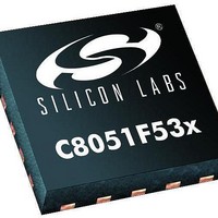
C8051F530-TB Silicon Laboratories Inc, C8051F530-TB Datasheet - Page 36

C8051F530-TB
Manufacturer Part Number
C8051F530-TB
Description
BOARD PROTOTYPE W/C8051F530
Manufacturer
Silicon Laboratories Inc
Type
MCUr
Datasheet
1.C8051F530-TB.pdf
(218 pages)
Specifications of C8051F530-TB
Contents
Board
Processor To Be Evaluated
C8051F52xA and C8051F53xA
Interface Type
USB
Lead Free Status / RoHS Status
Vendor undefined / Vendor undefined
For Use With/related Products
C8051F530
Lead Free Status / Rohs Status
Lead free / RoHS Compliant
- Current page: 36 of 218
- Download datasheet (2Mb)
C8051F52x/F52xA/F53x/F53xA
Table 3.1. Pin Definitions for the C8051F52x and C8051F52xA (DFN 10)
36
Note: Please refer to Section “20. Device Specific Behavior” on page 209.
P0.5/RX*/
CNVSTR
CNVSTR
P0.4/RX*
P0.4/TX*
V
XTAL2
Name
C2CK
RST/
P0.0/
V
P0.5/
GND
P0.3
REGIN
V
REF
DD
‘F52xA ‘F52x
Pin Numbers
—
—
1
2
3
4
5
6
7
8
—
—
—
1
2
3
4
5
6
7
D I/O or
D I/O or
D I/O or
D I/O or
D I/O or
D I/O or
A O or
D I/O
D I/O
D I/O
Type
D In
D In
D In
A In
A In
A In
A In
A In
A In
Description
Device Reset. Open-drain output of internal POR or V
An external source can initiate a system reset by driving this pin
low for at least the minimum RST low time to generate a system
reset, as defined in Table 2.7 on page 32. A 1 k pullup to V
is recommended. See Reset Sources Section for a complete
description.
Clock signal for the C2 Debug Interface.
Port 0.0. See Port I/O Section for a complete description.
External V
Ground.
Core Supply Voltage.
On-Chip Voltage Regulator Input.
Port 0.5. See Port I/O Section for a complete description.
External Converter start input for the ADC0, see Section “4. 12-Bit
ADC (ADC0)” on page 52 for a complete description.
Port 0.5. See Port I/O Section for a complete description.
External Converter start input for the ADC0, see Section “4. 12-Bit
ADC (ADC0)” on page 52 for a complete description.
Port 0.4. See Port I/O Section for a complete description.
Port 0.4. See Port I/O Section for a complete description.
Port 0.3. See Port I/O Section for a complete description.
External Clock Output. For an external crystal or resonator, this pin
is the excitation driver. This pin is the external clock input for
CMOS, capacitor, or RC oscillator configurations. See Section
“14. Oscillators” on page 134.
Rev. 1.3
REF
Input. See V
REF
Section.
DD
monitor.
REGIN
Related parts for C8051F530-TB
Image
Part Number
Description
Manufacturer
Datasheet
Request
R
Part Number:
Description:
SMD/C°/SINGLE-ENDED OUTPUT SILICON OSCILLATOR
Manufacturer:
Silicon Laboratories Inc
Part Number:
Description:
Manufacturer:
Silicon Laboratories Inc
Datasheet:
Part Number:
Description:
N/A N/A/SI4010 AES KEYFOB DEMO WITH LCD RX
Manufacturer:
Silicon Laboratories Inc
Datasheet:
Part Number:
Description:
N/A N/A/SI4010 SIMPLIFIED KEY FOB DEMO WITH LED RX
Manufacturer:
Silicon Laboratories Inc
Datasheet:
Part Number:
Description:
N/A/-40 TO 85 OC/EZLINK MODULE; F930/4432 HIGH BAND (REV E/B1)
Manufacturer:
Silicon Laboratories Inc
Part Number:
Description:
EZLink Module; F930/4432 Low Band (rev e/B1)
Manufacturer:
Silicon Laboratories Inc
Part Number:
Description:
I°/4460 10 DBM RADIO TEST CARD 434 MHZ
Manufacturer:
Silicon Laboratories Inc
Part Number:
Description:
I°/4461 14 DBM RADIO TEST CARD 868 MHZ
Manufacturer:
Silicon Laboratories Inc
Part Number:
Description:
I°/4463 20 DBM RFSWITCH RADIO TEST CARD 460 MHZ
Manufacturer:
Silicon Laboratories Inc
Part Number:
Description:
I°/4463 20 DBM RADIO TEST CARD 868 MHZ
Manufacturer:
Silicon Laboratories Inc
Part Number:
Description:
I°/4463 27 DBM RADIO TEST CARD 868 MHZ
Manufacturer:
Silicon Laboratories Inc
Part Number:
Description:
I°/4463 SKYWORKS 30 DBM RADIO TEST CARD 915 MHZ
Manufacturer:
Silicon Laboratories Inc
Part Number:
Description:
N/A N/A/-40 TO 85 OC/4463 RFMD 30 DBM RADIO TEST CARD 915 MHZ
Manufacturer:
Silicon Laboratories Inc
Part Number:
Description:
I°/4463 20 DBM RADIO TEST CARD 169 MHZ
Manufacturer:
Silicon Laboratories Inc


