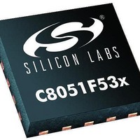
C8051F530-TB Silicon Laboratories Inc, C8051F530-TB Datasheet - Page 108

C8051F530-TB
Manufacturer Part Number
C8051F530-TB
Description
BOARD PROTOTYPE W/C8051F530
Manufacturer
Silicon Laboratories Inc
Type
MCUr
Datasheet
1.C8051F530-TB.pdf
(218 pages)
Specifications of C8051F530-TB
Contents
Board
Processor To Be Evaluated
C8051F52xA and C8051F53xA
Interface Type
USB
Lead Free Status / RoHS Status
Vendor undefined / Vendor undefined
For Use With/related Products
C8051F530
Lead Free Status / Rohs Status
Lead free / RoHS Compliant
- Current page: 108 of 218
- Download datasheet (2Mb)
C8051F52x/F52xA/F53x/F53xA
software, and a software reset is performed, the V
tect the integrity of Flash contents, the V
(VDMLVL = '1') and selected as a reset source if software contains routines which erase or write
Flash memory. If the V
will cause a Flash Error device reset.
The V
as a reset source before it is enabled and stabilized may cause a system reset. The procedure for re-
enabling the V
1. Enable the V
2. Wait for the V
3. Select the V
See Figure 11.2 for V
See Table 2.7 on page 32 for complete electrical characteristics of the V
Note: Software should take care not to inadvertently disable the V
ing to RSTSRC to enable other reset sources or to trigger a software reset. All writes to RSTSRC should
explicitly set PORSF to '1' to keep the V
Note: The output of the internal voltage regulator is calibrated by the MCU immediately after any reset
event. The output of the un-calibrated internal regulator could be below the high threshold setting of the
VDD Monitor. If this is the case and the VDD Monitor is set to the high threshold setting and if the MCU
receives a non-power on reset (POR), the MCU will remain in reset until a POR occurs (i.e. VDD Monitor
will keep the device in reset). A POR will force the VDD Monitor to the low threshold setting which is guar-
anteed to be below the un-calibrated output of the internal regulator. The device will then exit reset and
resume normal operation. It is for this reason Silicon Labs strongly recommends that the VDD Monitor is
always left in the low threshold setting (i.e., default value upon POR).
When programming the Flash in-system, the VDD Monitor must be set to the high threshold setting. For
the highest system reliability, the time the VDD Monitor is set to the high threshold setting should be mini-
mized (e.g., setting the VDD Monitor to the high threshold setting just before the Flash write operation and
then changing it back to the low threshold setting immediately after the Flash write operation).
108
This delay should be omitted if software contains routines which write or erase Flash memory.
DD
monitor must be enabled before it is selected as a reset source. Selecting the V
DD
DD
DD
DD
monitor and configuring the V
monitor as a reset source (PORSF bit in RSTSRC = 1).
monitor (VDMEN bit in VDDMON = 1).
monitor to stabilize (see Table 2.7 on page 32 for the V
DD
DD
monitor timing; note that the reset delay is not incurred after a V
monitor is not enabled, any erase or write performed on Flash memory
DD
Monitor enabled as a reset source.
DD
DD
Rev. 1.3
monitor as a reset source is shown below:
DD
monitor must be enabled to the higher setting
monitor will still be disabled after the reset. To pro-
DD
Monitor as a reset source when writ-
DD
DD
monitor.
Monitor turn-on time). Note:
DD
monitor reset.
DD
monitor
Related parts for C8051F530-TB
Image
Part Number
Description
Manufacturer
Datasheet
Request
R
Part Number:
Description:
SMD/C°/SINGLE-ENDED OUTPUT SILICON OSCILLATOR
Manufacturer:
Silicon Laboratories Inc
Part Number:
Description:
Manufacturer:
Silicon Laboratories Inc
Datasheet:
Part Number:
Description:
N/A N/A/SI4010 AES KEYFOB DEMO WITH LCD RX
Manufacturer:
Silicon Laboratories Inc
Datasheet:
Part Number:
Description:
N/A N/A/SI4010 SIMPLIFIED KEY FOB DEMO WITH LED RX
Manufacturer:
Silicon Laboratories Inc
Datasheet:
Part Number:
Description:
N/A/-40 TO 85 OC/EZLINK MODULE; F930/4432 HIGH BAND (REV E/B1)
Manufacturer:
Silicon Laboratories Inc
Part Number:
Description:
EZLink Module; F930/4432 Low Band (rev e/B1)
Manufacturer:
Silicon Laboratories Inc
Part Number:
Description:
I°/4460 10 DBM RADIO TEST CARD 434 MHZ
Manufacturer:
Silicon Laboratories Inc
Part Number:
Description:
I°/4461 14 DBM RADIO TEST CARD 868 MHZ
Manufacturer:
Silicon Laboratories Inc
Part Number:
Description:
I°/4463 20 DBM RFSWITCH RADIO TEST CARD 460 MHZ
Manufacturer:
Silicon Laboratories Inc
Part Number:
Description:
I°/4463 20 DBM RADIO TEST CARD 868 MHZ
Manufacturer:
Silicon Laboratories Inc
Part Number:
Description:
I°/4463 27 DBM RADIO TEST CARD 868 MHZ
Manufacturer:
Silicon Laboratories Inc
Part Number:
Description:
I°/4463 SKYWORKS 30 DBM RADIO TEST CARD 915 MHZ
Manufacturer:
Silicon Laboratories Inc
Part Number:
Description:
N/A N/A/-40 TO 85 OC/4463 RFMD 30 DBM RADIO TEST CARD 915 MHZ
Manufacturer:
Silicon Laboratories Inc
Part Number:
Description:
I°/4463 20 DBM RADIO TEST CARD 169 MHZ
Manufacturer:
Silicon Laboratories Inc


