C8051F411EK Silicon Laboratories Inc, C8051F411EK Datasheet - Page 70
C8051F411EK
Manufacturer Part Number
C8051F411EK
Description
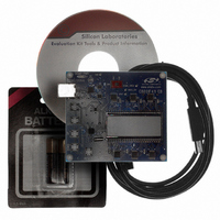
KIT EVAL FOR C8051F411
Manufacturer
Silicon Laboratories Inc
Type
MCUr
Specifications of C8051F411EK
Contents
Evaluation Board, CD-ROM, USB Cable, Batteries and User Guide
Processor To Be Evaluated
C8051F41x
Interface Type
USB
Silicon Manufacturer
Silicon Labs
Core Architecture
8051
Silicon Core Number
C8051F411
Silicon Family Name
C8051F41x
Kit Contents
LCD Based Evaluation Board, USB Cable, Software CD And Quick-Start Guide
Lead Free Status / RoHS Status
Contains lead / RoHS non-compliant
For Use With/related Products
Silicon Laboratories C8051F41x
For Use With
336-1315 - KIT REF DESIGN VOICE RECORD F41X
Lead Free Status / Rohs Status
Lead free / RoHS Compliant
Other names
336-1317


C8051F410/1/2/3
6.1.2. Update Output Based on Timer Overflow
The IDAC output update can be scheduled on a Timer overflow. This feature is useful in systems where the
IDAC is used to generate a waveform of a defined sampling rate, by eliminating the effects of variable
interrupt latency and instruction execution on the timing of the IDAC output. When the IDAnCM bits
(IDAnCN.[6:4]) are set to ‘000’, ‘001’, ‘010’ or ‘011’, writes to both IDAC data registers (IDAnL and IDAnH)
are held until an associated Timer overflow event (Timer 0, Timer 1, Timer 2 or Timer 3, respectively)
occurs, at which time the IDAnH:IDAnL contents are copied to the IDAC input latch, allowing the IDAC out-
put to change to the new value. When updates are scheduled based on Timer 2 or 3, updates occur on
low-byte overflows if Timer 2 or 3 is in 8-bit mode and high-byte overflows if Timer 2 or 3 is in 16-bit mode.
6.1.3. Update Output Based on CNVSTR Edge
The IDAC output can also be configured to update on a rising edge, falling edge, or both edges of the
external CNVSTR signal. When the IDAnCM bits (IDAnCN.[6:4]) are set to ‘100’, ‘101’, or ‘110’, writes to
the IDAC data registers (IDAnL and IDAnH) are held until an edge occurs on the CNVSTR input pin. The
particular setting of the IDAnCM bits determines whether the IDAC output is updated on rising, falling, or
both edges of CNVSTR. When a corresponding edge occurs, the IDAnH:IDAnL contents are copied to the
IDAC input latch, allowing the IDAC output to change to the new value.
6.2.
The IDAC data word can be Left Justified or Right Justified as shown in Figure 6.2. When Left Justified, the
8 MSBs of the data word (D11-D4) are mapped to bits 7-0 of the IDAnH register and the 4 LSBs of the data
word (D3-D0) are mapped to bits 7-4 of the IDAnL register. When Right Justified, the 4 MSBs of the data
word (D11-D8) are mapped to bits 3-0 of the IDAnH register and the 8 LSBs of the data word (D7-D0) are
mapped to bits 7-0 of the IDAnL register. The IDAC data word justification is selected using the IDAnRJST
bit (IDAnCN.2).
The full-scale output current of the IDAC is selected using the IDAnOMD bits (IDAnCN[1:0]). By default,
the IDAC is set to a full-scale output current of 2 mA. The IDAnOMD bits can also be configured to provide
full-scale output currents of 0.25 mA, 0.5 mA, or 1 mA.
70
Left Justified Data (IDAnRJST = 0):
Right Justified Data (IDAnRJST = 1):
IDAn Data Word
D11
(D11–D0)
IDAC Output Mapping
0xFFF
0x000
0x001
0x800
D10
D9
2048/4096 x 2 mA 2048/4096 x 1 mA 2048/4096 x 0.5 mA 2048/4096 x 0.25 mA
4095/4096 x 2 mA 4095/4096 x 1 mA 4095/4096 x 0.5 mA 4095/4096 x 0.25 mA
D8
1/4096 x 2 mA
IDAnH
IDAnH
‘11’ (2 mA)
0 mA
Figure 6.2. IDAC Data Word Mapping
D11
D7
D10
D6
Output Current vs IDAnOMD bit setting
D5
D9
1/4096 x 1 mA
‘10’ (1 mA)
0 mA
D4
D8
Rev. 1.1
D3
D7
D2
D6
1/4096 x 0.5 mA
‘01’ (0.5 mA)
D1
D5
0 mA
D0
D4
IDAnL
IDAnL
D3
1/4096 x 0.25 mA
‘00’ (0.25 mA)
D2
0 mA
D1
D0
Related parts for C8051F411EK
Image
Part Number
Description
Manufacturer
Datasheet
Request
R

Part Number:
Description:
SMD/C°/SINGLE-ENDED OUTPUT SILICON OSCILLATOR
Manufacturer:
Silicon Laboratories Inc
Part Number:
Description:
Manufacturer:
Silicon Laboratories Inc
Datasheet:
Part Number:
Description:
N/A N/A/SI4010 AES KEYFOB DEMO WITH LCD RX
Manufacturer:
Silicon Laboratories Inc
Datasheet:
Part Number:
Description:
N/A N/A/SI4010 SIMPLIFIED KEY FOB DEMO WITH LED RX
Manufacturer:
Silicon Laboratories Inc
Datasheet:
Part Number:
Description:
N/A/-40 TO 85 OC/EZLINK MODULE; F930/4432 HIGH BAND (REV E/B1)
Manufacturer:
Silicon Laboratories Inc
Part Number:
Description:
EZLink Module; F930/4432 Low Band (rev e/B1)
Manufacturer:
Silicon Laboratories Inc
Part Number:
Description:
I°/4460 10 DBM RADIO TEST CARD 434 MHZ
Manufacturer:
Silicon Laboratories Inc
Part Number:
Description:
I°/4461 14 DBM RADIO TEST CARD 868 MHZ
Manufacturer:
Silicon Laboratories Inc
Part Number:
Description:
I°/4463 20 DBM RFSWITCH RADIO TEST CARD 460 MHZ
Manufacturer:
Silicon Laboratories Inc
Part Number:
Description:
I°/4463 20 DBM RADIO TEST CARD 868 MHZ
Manufacturer:
Silicon Laboratories Inc
Part Number:
Description:
I°/4463 27 DBM RADIO TEST CARD 868 MHZ
Manufacturer:
Silicon Laboratories Inc
Part Number:
Description:
I°/4463 SKYWORKS 30 DBM RADIO TEST CARD 915 MHZ
Manufacturer:
Silicon Laboratories Inc
Part Number:
Description:
N/A N/A/-40 TO 85 OC/4463 RFMD 30 DBM RADIO TEST CARD 915 MHZ
Manufacturer:
Silicon Laboratories Inc
Part Number:
Description:
I°/4463 20 DBM RADIO TEST CARD 169 MHZ
Manufacturer:
Silicon Laboratories Inc