C8051F411EK Silicon Laboratories Inc, C8051F411EK Datasheet - Page 60
C8051F411EK
Manufacturer Part Number
C8051F411EK
Description
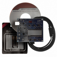
KIT EVAL FOR C8051F411
Manufacturer
Silicon Laboratories Inc
Type
MCUr
Specifications of C8051F411EK
Contents
Evaluation Board, CD-ROM, USB Cable, Batteries and User Guide
Processor To Be Evaluated
C8051F41x
Interface Type
USB
Silicon Manufacturer
Silicon Labs
Core Architecture
8051
Silicon Core Number
C8051F411
Silicon Family Name
C8051F41x
Kit Contents
LCD Based Evaluation Board, USB Cable, Software CD And Quick-Start Guide
Lead Free Status / RoHS Status
Contains lead / RoHS non-compliant
For Use With/related Products
Silicon Laboratories C8051F41x
For Use With
336-1315 - KIT REF DESIGN VOICE RECORD F41X
Lead Free Status / Rohs Status
Lead free / RoHS Compliant
Other names
336-1317


C8051F410/1/2/3
60
Bits7–3: AD0SC4–0: ADC0 SAR Conversion Clock Period Bits.
Bits2–1: AD0RPT1–0: ADC0 Repeat Count.
Bit0:
R/W
Bit7
SAR Conversion clock is derived from FCLK by the following equation, where AD0SC refers
to the 5-bit value held in bits AD0SC4-0. SAR Conversion clock requirements are given in
Table 5.3.
BURSTEN = 0: FCLK is the current system clock.
BURSTEN = 1: FCLK is a maximum of 25 MHz, independent of the current system clock.
*Note: Round the result up.
Controls the number of conversions taken and accumulated between ADC0 End of
Conversion (ADCINT) and ADC0 Window Comparator (ADCWINT) interrupts. A convert
start is required for each conversion unless Burst Mode is enabled. In Burst Mode, a single
convert start can initiate multiple self-timed conversions. Results in both modes are
accumulated in the ADC0H:ADC0L register. When AD0RPT1-0 are set to a value other
than '00', the AD0LJST bit in the ADC0CN register must be set to '0' (right justified).
00: 1 conversion is performed.
01: 4 conversions are performed and accumulated.
10: 8 conversions are performed and accumulated.
11: 16 conversions are performed and accumulated.
Note:
RESERVED. Read = 0b; Must write 0b.
AD0SC
R/W
Bit6
The ADC0 output register is automatically reset to 0x0000 upon reaching the last conversion
specified by the repeat counter. If the ADC is disabled during a conversion and re-enabled later,
the ADC0H and ADC0L registers should be manually cleared to 0x00.
SFR Definition 5.2. ADC0CF: ADC0 Configuration
=
------------------- - 1
CLK
AD0SC
FCLK
R/W
Bit5
SAR
–
*
R/W
Bit4
or
Rev. 1.1
R/W
Bit3
CLK
SAR
R/W
Bit2
=
AD0RPT
----------------------------
AD0SC
FCLK
R/W
Bit1
+
1
Reserved 11111000
R/W
Bit0
SFR Address:
Reset Value
0xBC
Related parts for C8051F411EK
Image
Part Number
Description
Manufacturer
Datasheet
Request
R

Part Number:
Description:
SMD/C°/SINGLE-ENDED OUTPUT SILICON OSCILLATOR
Manufacturer:
Silicon Laboratories Inc
Part Number:
Description:
Manufacturer:
Silicon Laboratories Inc
Datasheet:
Part Number:
Description:
N/A N/A/SI4010 AES KEYFOB DEMO WITH LCD RX
Manufacturer:
Silicon Laboratories Inc
Datasheet:
Part Number:
Description:
N/A N/A/SI4010 SIMPLIFIED KEY FOB DEMO WITH LED RX
Manufacturer:
Silicon Laboratories Inc
Datasheet:
Part Number:
Description:
N/A/-40 TO 85 OC/EZLINK MODULE; F930/4432 HIGH BAND (REV E/B1)
Manufacturer:
Silicon Laboratories Inc
Part Number:
Description:
EZLink Module; F930/4432 Low Band (rev e/B1)
Manufacturer:
Silicon Laboratories Inc
Part Number:
Description:
I°/4460 10 DBM RADIO TEST CARD 434 MHZ
Manufacturer:
Silicon Laboratories Inc
Part Number:
Description:
I°/4461 14 DBM RADIO TEST CARD 868 MHZ
Manufacturer:
Silicon Laboratories Inc
Part Number:
Description:
I°/4463 20 DBM RFSWITCH RADIO TEST CARD 460 MHZ
Manufacturer:
Silicon Laboratories Inc
Part Number:
Description:
I°/4463 20 DBM RADIO TEST CARD 868 MHZ
Manufacturer:
Silicon Laboratories Inc
Part Number:
Description:
I°/4463 27 DBM RADIO TEST CARD 868 MHZ
Manufacturer:
Silicon Laboratories Inc
Part Number:
Description:
I°/4463 SKYWORKS 30 DBM RADIO TEST CARD 915 MHZ
Manufacturer:
Silicon Laboratories Inc
Part Number:
Description:
N/A N/A/-40 TO 85 OC/4463 RFMD 30 DBM RADIO TEST CARD 915 MHZ
Manufacturer:
Silicon Laboratories Inc
Part Number:
Description:
I°/4463 20 DBM RADIO TEST CARD 169 MHZ
Manufacturer:
Silicon Laboratories Inc