C8051F411EK Silicon Laboratories Inc, C8051F411EK Datasheet - Page 222
C8051F411EK
Manufacturer Part Number
C8051F411EK
Description
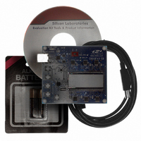
KIT EVAL FOR C8051F411
Manufacturer
Silicon Laboratories Inc
Type
MCUr
Specifications of C8051F411EK
Contents
Evaluation Board, CD-ROM, USB Cable, Batteries and User Guide
Processor To Be Evaluated
C8051F41x
Interface Type
USB
Silicon Manufacturer
Silicon Labs
Core Architecture
8051
Silicon Core Number
C8051F411
Silicon Family Name
C8051F41x
Kit Contents
LCD Based Evaluation Board, USB Cable, Software CD And Quick-Start Guide
Lead Free Status / RoHS Status
Contains lead / RoHS non-compliant
For Use With/related Products
Silicon Laboratories C8051F41x
For Use With
336-1315 - KIT REF DESIGN VOICE RECORD F41X
Lead Free Status / Rohs Status
Lead free / RoHS Compliant
Other names
336-1317


C8051F410/1/2/3
whichever is slower. When the SPI is configured as a slave, the maximum data transfer rate (bits/sec) for
full-duplex operation is 1/10 the system clock frequency, provided that the master issues SCK, NSS (in 4-
wire slave mode), and the serial input data synchronously with the slave’s system clock. If the master
issues SCK, NSS, and the serial input data asynchronously, the maximum data transfer rate (bits/sec)
must be less than 1/10 the system clock frequency. In the special case where the master only wants to
transmit data to the slave and does not need to receive data from the slave (i.e. half-duplex operation), the
SPI slave can receive data at a maximum data transfer rate (bits/sec) of 1/4 the system clock frequency.
This is provided that the master issues SCK, NSS, and the serial input data synchronously with the slave’s
system clock.
23.6. SPI Special Function Registers
SPI0 is accessed and controlled through four special function registers in the system controller: SPI0CN
Control Register, SPI0DAT Data Register, SPI0CFG Configuration Register, and SPI0CKR Clock Rate
Register. The four special function registers related to the operation of the SPI0 Bus are described in the
following figures.
222
SCK
(CKPOL=0, CKPHA=0)
SCK
(CKPOL=0, CKPHA=1)
SCK
(CKPOL=1, CKPHA=0)
SCK
(CKPOL=1, CKPHA=1)
MISO/MOSI
Figure 23.5. Data/Clock Timing Relationship
MSB
Bit 6
Bit 5
Rev. 1.1
Bit 4
Bit 3
Bit 2
Bit 1
Bit 0
Related parts for C8051F411EK
Image
Part Number
Description
Manufacturer
Datasheet
Request
R

Part Number:
Description:
SMD/C°/SINGLE-ENDED OUTPUT SILICON OSCILLATOR
Manufacturer:
Silicon Laboratories Inc
Part Number:
Description:
Manufacturer:
Silicon Laboratories Inc
Datasheet:
Part Number:
Description:
N/A N/A/SI4010 AES KEYFOB DEMO WITH LCD RX
Manufacturer:
Silicon Laboratories Inc
Datasheet:
Part Number:
Description:
N/A N/A/SI4010 SIMPLIFIED KEY FOB DEMO WITH LED RX
Manufacturer:
Silicon Laboratories Inc
Datasheet:
Part Number:
Description:
N/A/-40 TO 85 OC/EZLINK MODULE; F930/4432 HIGH BAND (REV E/B1)
Manufacturer:
Silicon Laboratories Inc
Part Number:
Description:
EZLink Module; F930/4432 Low Band (rev e/B1)
Manufacturer:
Silicon Laboratories Inc
Part Number:
Description:
I°/4460 10 DBM RADIO TEST CARD 434 MHZ
Manufacturer:
Silicon Laboratories Inc
Part Number:
Description:
I°/4461 14 DBM RADIO TEST CARD 868 MHZ
Manufacturer:
Silicon Laboratories Inc
Part Number:
Description:
I°/4463 20 DBM RFSWITCH RADIO TEST CARD 460 MHZ
Manufacturer:
Silicon Laboratories Inc
Part Number:
Description:
I°/4463 20 DBM RADIO TEST CARD 868 MHZ
Manufacturer:
Silicon Laboratories Inc
Part Number:
Description:
I°/4463 27 DBM RADIO TEST CARD 868 MHZ
Manufacturer:
Silicon Laboratories Inc
Part Number:
Description:
I°/4463 SKYWORKS 30 DBM RADIO TEST CARD 915 MHZ
Manufacturer:
Silicon Laboratories Inc
Part Number:
Description:
N/A N/A/-40 TO 85 OC/4463 RFMD 30 DBM RADIO TEST CARD 915 MHZ
Manufacturer:
Silicon Laboratories Inc
Part Number:
Description:
I°/4463 20 DBM RADIO TEST CARD 169 MHZ
Manufacturer:
Silicon Laboratories Inc