C8051F411EK Silicon Laboratories Inc, C8051F411EK Datasheet - Page 69
C8051F411EK
Manufacturer Part Number
C8051F411EK
Description
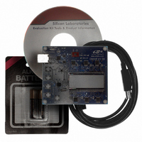
KIT EVAL FOR C8051F411
Manufacturer
Silicon Laboratories Inc
Type
MCUr
Specifications of C8051F411EK
Contents
Evaluation Board, CD-ROM, USB Cable, Batteries and User Guide
Processor To Be Evaluated
C8051F41x
Interface Type
USB
Silicon Manufacturer
Silicon Labs
Core Architecture
8051
Silicon Core Number
C8051F411
Silicon Family Name
C8051F41x
Kit Contents
LCD Based Evaluation Board, USB Cable, Software CD And Quick-Start Guide
Lead Free Status / RoHS Status
Contains lead / RoHS non-compliant
For Use With/related Products
Silicon Laboratories C8051F41x
For Use With
336-1315 - KIT REF DESIGN VOICE RECORD F41X
Lead Free Status / Rohs Status
Lead free / RoHS Compliant
Other names
336-1317


6.
The C8051F41x devices include two 12-bit current-mode Digital-to-Analog Converters (IDACs). The maxi-
mum current output of the IDACs can be adjusted for four different current settings; 0.25 mA, 0.5 mA,
1 mA, and 2 mA. The IDACs can be individually enabled or disabled using the enable bits in the corre-
sponding IDAC Control Register (IDA0CN or IDA1CN). When both IDACs are enabled, their outputs may
be routed to individual pins or merged onto a single pin. An internal bandgap bias generator is used to gen-
erate a reference current for the IDACs whenever they are enabled. IDAC updates can be performed on-
demand, scheduled on a Timer overflow, or synchronized with an external pin edge. Figure 6.1 shows a
block diagram of the IDAC circuitry.
6.1.
A flexible output update mechanism allows for seamless full-scale changes and supports jitter-free
updates for waveform generation. Three update modes are provided, allowing IDAC output updates on a
write to the IDAC’s data register, on a Timer overflow, or on an external pin edge.
6.1.1. Update Output On-Demand
In its default mode (IDAnCN.[6:4] = ‘111’) the IDAC output is updated “on-demand” with a write to the data
register high byte (IDAnH). It is important to note that in this mode, writes to the data register low byte
(IDAnL) are held and have no effect on the IDAn output until a write to IDAnH takes place. Since data from
both the high and low bytes of the data register are immediately latched to IDAn after a write to IDAnH, the
write sequence when writing a full 12-bit word to the IDAC data registers should be IDAnL followed
by IDAnH . When the data word is left justified, the IDAC can be used in 8-bit mode by initializing IDAnL to
the desired value (typically 0x00), and writing data only to IDA0H.
12-Bit Current Mode DACs (IDA0 and IDA1)
IDAC Output Scheduling
IDAnOMD1
IDAnOMD0
IDAnRJST
IDAnCM2
IDAnCM1
IDAnCM0
IDAnEN
Figure 6.1. IDAC Functional Block Diagram
8
4
Rev. 1.1
12
IDAn
C8051F410/1/2/3
IDAn
Output
69
Related parts for C8051F411EK
Image
Part Number
Description
Manufacturer
Datasheet
Request
R

Part Number:
Description:
SMD/C°/SINGLE-ENDED OUTPUT SILICON OSCILLATOR
Manufacturer:
Silicon Laboratories Inc
Part Number:
Description:
Manufacturer:
Silicon Laboratories Inc
Datasheet:
Part Number:
Description:
N/A N/A/SI4010 AES KEYFOB DEMO WITH LCD RX
Manufacturer:
Silicon Laboratories Inc
Datasheet:
Part Number:
Description:
N/A N/A/SI4010 SIMPLIFIED KEY FOB DEMO WITH LED RX
Manufacturer:
Silicon Laboratories Inc
Datasheet:
Part Number:
Description:
N/A/-40 TO 85 OC/EZLINK MODULE; F930/4432 HIGH BAND (REV E/B1)
Manufacturer:
Silicon Laboratories Inc
Part Number:
Description:
EZLink Module; F930/4432 Low Band (rev e/B1)
Manufacturer:
Silicon Laboratories Inc
Part Number:
Description:
I°/4460 10 DBM RADIO TEST CARD 434 MHZ
Manufacturer:
Silicon Laboratories Inc
Part Number:
Description:
I°/4461 14 DBM RADIO TEST CARD 868 MHZ
Manufacturer:
Silicon Laboratories Inc
Part Number:
Description:
I°/4463 20 DBM RFSWITCH RADIO TEST CARD 460 MHZ
Manufacturer:
Silicon Laboratories Inc
Part Number:
Description:
I°/4463 20 DBM RADIO TEST CARD 868 MHZ
Manufacturer:
Silicon Laboratories Inc
Part Number:
Description:
I°/4463 27 DBM RADIO TEST CARD 868 MHZ
Manufacturer:
Silicon Laboratories Inc
Part Number:
Description:
I°/4463 SKYWORKS 30 DBM RADIO TEST CARD 915 MHZ
Manufacturer:
Silicon Laboratories Inc
Part Number:
Description:
N/A N/A/-40 TO 85 OC/4463 RFMD 30 DBM RADIO TEST CARD 915 MHZ
Manufacturer:
Silicon Laboratories Inc
Part Number:
Description:
I°/4463 20 DBM RADIO TEST CARD 169 MHZ
Manufacturer:
Silicon Laboratories Inc