C8051F411EK Silicon Laboratories Inc, C8051F411EK Datasheet - Page 11
C8051F411EK
Manufacturer Part Number
C8051F411EK
Description
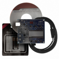
KIT EVAL FOR C8051F411
Manufacturer
Silicon Laboratories Inc
Type
MCUr
Specifications of C8051F411EK
Contents
Evaluation Board, CD-ROM, USB Cable, Batteries and User Guide
Processor To Be Evaluated
C8051F41x
Interface Type
USB
Silicon Manufacturer
Silicon Labs
Core Architecture
8051
Silicon Core Number
C8051F411
Silicon Family Name
C8051F41x
Kit Contents
LCD Based Evaluation Board, USB Cable, Software CD And Quick-Start Guide
Lead Free Status / RoHS Status
Contains lead / RoHS non-compliant
For Use With/related Products
Silicon Laboratories C8051F41x
For Use With
336-1315 - KIT REF DESIGN VOICE RECORD F41X
Lead Free Status / Rohs Status
Lead free / RoHS Compliant
Other names
336-1317


23. Enhanced Serial Peripheral Interface (SPI0)
24. Timers
25. Programmable Counter Array (PCA0)
26. C2 Interface
Figure 23.1. SPI Block Diagram ............................................................................. 217
Figure 23.2. Multiple-Master Mode Connection Diagram ....................................... 220
Figure 23.3. 3-Wire Single Master and Slave Mode Connection Diagram ............. 220
Figure 23.4. 4-Wire Single Master and Slave Mode Connection Diagram ............. 220
Figure 23.5. Data/Clock Timing Relationship ......................................................... 222
Figure 23.6. SPI Master Timing (CKPHA = 0)........................................................ 227
Figure 23.7. SPI Master Timing (CKPHA = 1)........................................................ 227
Figure 23.8. SPI Slave Timing (CKPHA = 0).......................................................... 228
Figure 23.9. SPI Slave Timing (CKPHA = 1).......................................................... 228
Figure 24.1. T0 Mode 0 Block Diagram.................................................................. 232
Figure 24.2. T0 Mode 2 Block Diagram.................................................................. 233
Figure 24.3. T0 Mode 3 Block Diagram.................................................................. 234
Figure 24.4. Timer 2 16-Bit Mode Block Diagram .................................................. 239
Figure 24.5. Timer 2 8-Bit Mode Block Diagram .................................................... 240
Figure 24.6. Timer 2 Capture Mode Block Diagram ............................................... 241
Figure 24.7. Timer 3 16-Bit Mode Block Diagram .................................................. 244
Figure 24.8. Timer 3 8-Bit Mode Block Diagram .................................................... 245
Figure 24.9. Timer 3 Capture Mode Block Diagram ............................................... 246
Figure 25.1. PCA Block Diagram............................................................................ 249
Figure 25.2. PCA Counter/Timer Block Diagram.................................................... 250
Figure 25.3. PCA Interrupt Block Diagram ............................................................. 251
Figure 25.4. PCA Capture Mode Diagram.............................................................. 252
Figure 25.5. PCA Software Timer Mode Diagram .................................................. 253
Figure 25.6. PCA High-Speed Output Mode Diagram............................................ 254
Figure 25.7. PCA Frequency Output Mode ............................................................ 255
Figure 25.8. PCA 8-Bit PWM Mode Diagram ......................................................... 256
Figure 25.9. PCA 16-Bit PWM Mode...................................................................... 257
Figure 25.10. PCA Module 5 with Watchdog Timer Enabled ................................. 258
Figure 26.1. Typical C2 Pin Sharing....................................................................... 267
Rev. 1.1
C8051F410/1/2/3
11
Related parts for C8051F411EK
Image
Part Number
Description
Manufacturer
Datasheet
Request
R

Part Number:
Description:
SMD/C°/SINGLE-ENDED OUTPUT SILICON OSCILLATOR
Manufacturer:
Silicon Laboratories Inc
Part Number:
Description:
Manufacturer:
Silicon Laboratories Inc
Datasheet:
Part Number:
Description:
N/A N/A/SI4010 AES KEYFOB DEMO WITH LCD RX
Manufacturer:
Silicon Laboratories Inc
Datasheet:
Part Number:
Description:
N/A N/A/SI4010 SIMPLIFIED KEY FOB DEMO WITH LED RX
Manufacturer:
Silicon Laboratories Inc
Datasheet:
Part Number:
Description:
N/A/-40 TO 85 OC/EZLINK MODULE; F930/4432 HIGH BAND (REV E/B1)
Manufacturer:
Silicon Laboratories Inc
Part Number:
Description:
EZLink Module; F930/4432 Low Band (rev e/B1)
Manufacturer:
Silicon Laboratories Inc
Part Number:
Description:
I°/4460 10 DBM RADIO TEST CARD 434 MHZ
Manufacturer:
Silicon Laboratories Inc
Part Number:
Description:
I°/4461 14 DBM RADIO TEST CARD 868 MHZ
Manufacturer:
Silicon Laboratories Inc
Part Number:
Description:
I°/4463 20 DBM RFSWITCH RADIO TEST CARD 460 MHZ
Manufacturer:
Silicon Laboratories Inc
Part Number:
Description:
I°/4463 20 DBM RADIO TEST CARD 868 MHZ
Manufacturer:
Silicon Laboratories Inc
Part Number:
Description:
I°/4463 27 DBM RADIO TEST CARD 868 MHZ
Manufacturer:
Silicon Laboratories Inc
Part Number:
Description:
I°/4463 SKYWORKS 30 DBM RADIO TEST CARD 915 MHZ
Manufacturer:
Silicon Laboratories Inc
Part Number:
Description:
N/A N/A/-40 TO 85 OC/4463 RFMD 30 DBM RADIO TEST CARD 915 MHZ
Manufacturer:
Silicon Laboratories Inc
Part Number:
Description:
I°/4463 20 DBM RADIO TEST CARD 169 MHZ
Manufacturer:
Silicon Laboratories Inc