Z8F083A0128ZCOG Zilog, Z8F083A0128ZCOG Datasheet - Page 134
Z8F083A0128ZCOG
Manufacturer Part Number
Z8F083A0128ZCOG
Description
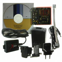
KIT DEVELOPMENT F083A
Manufacturer
Zilog
Series
Z8 Encore! XP®r
Type
MCUr
Specifications of Z8F083A0128ZCOG
Contents
Hardware, Software and Documentation
For Use With/related Products
Z8F083A
For Use With
269-4661 - KIT ACC ETHERNET SMART CABLE
Lead Free Status / RoHS Status
Lead free / RoHS Compliant
Other names
269-4672
Available stocks
Company
Part Number
Manufacturer
Quantity
Price
Company:

Part Number:
Z8F083A0128ZCOG
Manufacturer:
Zilog
Quantity:
1


Table 79. Flash Option Bits at Program Memory Address 0000H
BITS
FIELD
RESET
R/W
ADDR
Note: U = Unchanged by Reset. R/W = Read/Write.
PS026308-1207
Flash Program Memory Address 0000H
WDT_RES WDT_AO
R/W
U
7
WDT_RES—Watchdog Timer reset
0 = Watchdog Timer time-out generates an interrupt request. Interrupts must be globally
enabled for the eZ8 CPU to acknowledge the interrupt request.
1 = Watchdog Timer time-out causes a system reset. This is the default setting for
unprogrammed (erased) Flash.
WDT_AO—Watchdog Timer always On
0 = On application of system power, Watchdog Timer is automatically enabled. Watchdog
Timer cannot be disabled.
1 = Watchdog Timer is enabled on execution of the WDT instruction. Once enabled, the
Watchdog Timer is disabled only by a reset. This is the default setting for unprogrammed
(erased) Flash.
OSC_SEL[1:0]—OSCILLATOR mode selection
00 = On-chip oscillator configured for use with external RC networks (<4 MHz).
01 = Minimum power for use with very low frequency crystals (32 kHz to 1.0 MHz).
10 = Medium power for use with medium frequency crystals or ceramic resonators
(0.5 MHz to 5.0 MHz).
11 = Maximum power for use with high frequency crystals (5.0 MHz to 20.0 MHz).
This is the default setting for unprogrammed (erased) Flash.
VBO_AO—Voltage Brownout protection always On
0 = VBO protection is disabled in STOP mode to reduce total power consumption.
1 = VBO protection is always enabled, even during STOP mode. This is the default setting
for unprogrammed (erased) Flash.
FRP—Flash read protect
0 = User program code is inaccessible. Limited control features are available through the
On-Chip Debugger.
1 = User program code is accessible. All On-Chip Debugger commands are enabled. This
is the default setting for unprogrammed (erased) Flash.
Reserved—Must be 1
R/W
U
6
R/W
OSC_SEL[1:0]
U
5
Program Memory 0000H
R/W
U
4
VBO_AO
R/W
U
3
FRP
R/W
Z8 Encore!
U
2
Product Specification
Reserved
R/W
U
1
®
F083A Series
Flash Option Bits
FWP
R/W
U
0
122
Related parts for Z8F083A0128ZCOG
Image
Part Number
Description
Manufacturer
Datasheet
Request
R

Part Number:
Description:
Communication Controllers, ZILOG INTELLIGENT PERIPHERAL CONTROLLER (ZIP)
Manufacturer:
Zilog, Inc.
Datasheet:

Part Number:
Description:
KIT DEV FOR Z8 ENCORE 16K TO 64K
Manufacturer:
Zilog
Datasheet:

Part Number:
Description:
KIT DEV Z8 ENCORE XP 28-PIN
Manufacturer:
Zilog
Datasheet:

Part Number:
Description:
DEV KIT FOR Z8 ENCORE 8K/4K
Manufacturer:
Zilog
Datasheet:

Part Number:
Description:
KIT DEV Z8 ENCORE XP 28-PIN
Manufacturer:
Zilog
Datasheet:

Part Number:
Description:
DEV KIT FOR Z8 ENCORE 4K TO 8K
Manufacturer:
Zilog
Datasheet:
Part Number:
Description:
CMOS Z8 microcontroller. ROM 16 Kbytes, RAM 256 bytes, speed 16 MHz, 32 lines I/O, 3.0V to 5.5V
Manufacturer:
Zilog, Inc.
Datasheet:
Part Number:
Description:
Low-cost microcontroller. 512 bytes ROM, 61 bytes RAM, 8 MHz
Manufacturer:
Zilog, Inc.
Datasheet:
Part Number:
Description:
Z8 4K OTP Microcontroller
Manufacturer:
Zilog, Inc.
Datasheet:
Part Number:
Description:
CMOS SUPER8 ROMLESS MCU
Manufacturer:
Zilog, Inc.
Datasheet:
Part Number:
Description:
SL1866 CMOSZ8 OTP Microcontroller
Manufacturer:
Zilog, Inc.
Datasheet:
Part Number:
Description:
SL1866 CMOSZ8 OTP Microcontroller
Manufacturer:
Zilog, Inc.
Datasheet:
Part Number:
Description:
OTP (KB) = 1, RAM = 125, Speed = 12, I/O = 14, 8-bit Timers = 2, Comm Interfaces Other Features = Por, LV Protect, Voltage = 4.5-5.5V
Manufacturer:
Zilog, Inc.
Datasheet:
Part Number:
Description:
Manufacturer:
Zilog, Inc.
Datasheet: