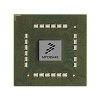
MPC8544DS Freescale Semiconductor, MPC8544DS Datasheet - Page 15

MPC8544DS
Manufacturer Part Number
MPC8544DS
Description
BOARD DEVELOPMENT SYSTEM 8544
Manufacturer
Freescale Semiconductor
Series
PowerQUICC III™r
Type
MPUr
Datasheets
1.MPC8544VTALF.pdf
(117 pages)
2.MPC8544VTALF.pdf
(2 pages)
3.MPC8544VTALF.pdf
(1340 pages)
4.MPC8544DS.pdf
(2 pages)
Specifications of MPC8544DS
Contents
Board
Processor To Be Evaluated
MPC8544E
Data Bus Width
32 bit
Interface Type
Ethernet, I2C
Operating Supply Voltage
- 0.3 V to + 1.1 V
Leaded Process Compatible
Yes
Peak Reflow Compatible (260 C)
Yes
Rohs Compliant
Yes
For Use With/related Products
MPC8544
For Use With
PPC8544EVTANG - EVAL MPC8544 783FCPBGA
Lead Free Status / RoHS Status
Lead free / RoHS Compliant
4.2
The RTC input is sampled by the platform clock (CCB clock). The output of the sampling latch is then
used as an input to the counters of the PIC and the TimeBase unit of the e500. There is no jitter
specification. The minimum pulse width of the RTC signal should be greater than 2 × the period of the
CCB clock. That is, minimum clock high time is 2 × t
is no minimum RTC frequency; RTC may be grounded if not needed.
4.3
Table 7
the MPC8544E.
4.4
Please note the following FIFO maximum speed restrictions based on platform speed.
For FIFO GMII mode:
For example, if the platform frequency is 533 MHz, the FIFO Tx/Rx clock frequency should be no more
than 127 MHz.
For FIFO encoded mode:
For example, if the platform frequency is 533 MHz, the FIFO Tx/Rx clock frequency should be no more
than 167 MHz.
Freescale Semiconductor
EC_GTX_CLK125 frequency
EC_GTX_CLK125 cycle time
EC_GTX_CLK rise and fall time
LV
LV
EC_GTX_CLK125 duty cycle
Notes:
1. Rise and fall times for EC_GTX_CLK125 are measured from 0.5 and 2.0 V for L/TV
2. EC_GTX_CLK125 is used to generate the GTX clock for the eTSEC transmitter with 2% degradation. EC_GTX_CLK125 duty
DD
DD
L/TVDD = 3.3 V.
cycle can be loosened from 47%/53% as long as the PHY device can tolerate the duty cycle generated by the eTSEC
GTX_CLK. See
reference clock.
, TV
, TV
FIFO TX/RX clock frequency ≤ platform clock frequency ÷ 4.2
FIFO TX/RX clock frequency ≤ platform clock frequency ÷ 3.2
provides the eTSEC gigabit reference clocks (EC_GTX_CLK125) AC timing specifications for
DD
DD
Real-Time Clock Timing
eTSEC Gigabit Reference Clock Timing
Platform to FIFO Restrictions
= 2.5 V
= 3.3 V
Parameter/Condition
1000Base-T for RGMII, RTBI
Section 8.7.4, “RGMII and RTBI AC Timing Specifications,”
MPC8544E PowerQUICC III Integrated Processor Hardware Specifications, Rev. 5
Table 7. EC_GTX_CLK125 AC Timing Specifications
GMII, TBI
t
G125R
t
G125H
Symbol
f
t
G125
G125
/t
/t
G125F
G125
CCB
, and minimum clock low time is 2 × t
Min
45
47
—
—
—
for duty cycle for 10Base-T and 100Base-T
Typ
125
—
—
8
DD
= 2.5 V, and from 0.6 and 2.7 V for
Max
0.75
1.0
55
53
—
—
MHz
Unit
ns
ns
%
CCB
Input Clocks
. There
Notes
—
—
1
2
15


