DK-DEV-2AGX125N Altera, DK-DEV-2AGX125N Datasheet - Page 82
DK-DEV-2AGX125N
Manufacturer Part Number
DK-DEV-2AGX125N
Description
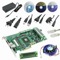
KIT DEV ARRIA II GX FPGA 2AGX125
Manufacturer
Altera
Series
Arria II GXr
Type
FPGAr
Datasheets
1.EP2AGX45CU17C6N.pdf
(96 pages)
2.DK-DEV-2AGX125N.pdf
(48 pages)
3.DK-DEV-2AGX125N.pdf
(64 pages)
Specifications of DK-DEV-2AGX125N
Contents
Board, Cables, CD, DVD, Power Supply
Silicon Manufacturer
Altera
Core Architecture
FPGA
Core Sub-architecture
Arria
Silicon Core Number
EP2
Silicon Family Name
Arria II GX
Rohs Compliant
Yes
For Use With/related Products
EP2AGX125EF35
Lead Free Status / RoHS Status
Lead free / RoHS Compliant
Other names
544-2600
Available stocks
Company
Part Number
Manufacturer
Quantity
Price
Company:

Part Number:
DK-DEV-2AGX125N
Manufacturer:
Altera
Quantity:
135


1–74
Table 1–58. DLL Frequency Range Specifications for Arria II GZ Devices (Part 2 of 2)
Table 1–61. Memory Output Clock Jitter Specification for Arria II GX Devices
Arria II Device Handbook Volume 3: Device Datasheet and Addendum
Note to
(1) Low indicates a 6-bit DQS delay setting; high indicates a 5-bit DQS delay setting.
Clock period jitter
Cycle-to-cycle period
jitter
Frequency Mode
Parameter
Table
7
1–58:
Table 1–59
Table 1–59. DQS Phase Offset Delay Per Setting for Arria II GX Devices
Table 1–60
Table 1–60. DQS Phase Shift Error Specification for DLL-Delayed Clock (t
Devices
Table 1–61
Notes to
(1) The valid settings for phase offset are -64 to +63 for frequency modes 0 to 3 and -32 to +31 for frequency modes
(2) The typical value equals the average of the minimum and maximum values.
(3) The delay settings are linear.
Note to
(1) This error specification is the absolute maximum and minimum error. For example, skew on three DQS delay
Network
470-630
Number of DQS Delay Buffer
Global
Global
Clock
4 to 5.
buffers in a 3 speed grade is ± 78 ps or ± 39 ps.
Frequency Range (MHz)
–3
Table
Table
(Note 1)
Speed Grade
lists the DQS phase offset delay per stage for Arria II GX devices.
lists the DQS phase shift error for Arria II GZ devices.
lists the memory output clock jitter specifications for Arria II GX devices.
I3, C5, I5
1–60:
1–59:
C4
C6
Symbol
1
2
3
4
t
t
JIT(per)
JIT(cc)
470-590
–4
-100
-200
Min
–4
Max
100
200
Available Phase Shift
60°, 120°, 180°, 240°
Min
7.0
7.0
8.5
112
–3
28
56
84
-125
-250
Min
(Note
Chapter 1: Device Datasheet for Arria II Devices
–5
Max
1), (2),
125
250
Max
13.0
15.0
18.0
December 2010 Altera Corporation
120
–4
30
60
90
Buffer Mode
(3)
DQS Delay
-125
-250
Min
(Note
DQS_PSERR
(Part 1 of 2)
High
(1)
Switching Characteristics
–6
1), (2),
) for Arria II GZ
Max
125
250
Unit
Number of
ps
ps
ps
(3)
Chains
Unit
Delay
ps
ps
ps
ps
6
Unit
ps
ps
Related parts for DK-DEV-2AGX125N
Image
Part Number
Description
Manufacturer
Datasheet
Request
R

Part Number:
Description:
KIT DEV CYCLONE III LS EP3CLS200
Manufacturer:
Altera
Datasheet:

Part Number:
Description:
KIT DEV STRATIX IV FPGA 4SE530
Manufacturer:
Altera
Datasheet:

Part Number:
Description:
KIT DEV FPGA 2AGX260 W/6.375G TX
Manufacturer:
Altera
Datasheet:

Part Number:
Description:
KIT DEV MAX V 5M570Z
Manufacturer:
Altera
Datasheet:

Part Number:
Description:
KIT DEV STRATIX V FPGA 5SGXEA7
Manufacturer:
Altera
Datasheet:

Part Number:
Description:
KIT DEVELOPMENT STRATIX III
Manufacturer:
Altera
Datasheet:

Part Number:
Description:
KIT DEVELOPMENT STRATIX IV
Manufacturer:
Altera
Datasheet:

Part Number:
Description:
KIT DEV ARRIA GX 1AGX60N
Manufacturer:
Altera
Datasheet:
Part Number:
Description:
KIT STARTER CYCLONE IV GX
Manufacturer:
Altera
Datasheet:
Part Number:
Description:
KIT DEVELOPMENT STRATIX IV
Manufacturer:
Altera
Datasheet:

Part Number:
Description:
CPLD, EP610 Family, ECMOS Process, 300 Gates, 16 Macro Cells, 16 Reg., 16 User I/Os, 5V Supply, 35 Speed Grade, 24DIP
Manufacturer:
Altera Corporation
Datasheet:
Part Number:
Description:
CPLD, EP610 Family, ECMOS Process, 300 Gates, 16 Macro Cells, 16 Reg., 16 User I/Os, 5V Supply, 15 Speed Grade, 24DIP
Manufacturer:
Altera Corporation
Datasheet: