DK-DEV-2AGX125N Altera, DK-DEV-2AGX125N Datasheet - Page 22
DK-DEV-2AGX125N
Manufacturer Part Number
DK-DEV-2AGX125N
Description
KIT DEV ARRIA II GX FPGA 2AGX125
Manufacturer
Altera
Series
Arria II GXr
Type
FPGAr
Datasheets
1.EP2AGX45CU17C6N.pdf
(96 pages)
2.DK-DEV-2AGX125N.pdf
(48 pages)
3.DK-DEV-2AGX125N.pdf
(64 pages)
Specifications of DK-DEV-2AGX125N
Contents
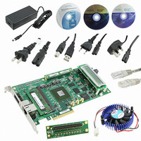
Board, Cables, CD, DVD, Power Supply
Silicon Manufacturer
Altera
Core Architecture
FPGA
Core Sub-architecture
Arria
Silicon Core Number
EP2
Silicon Family Name
Arria II GX
Rohs Compliant
Yes
For Use With/related Products
EP2AGX125EF35
Lead Free Status / RoHS Status
Lead free / RoHS Compliant
Other names
544-2600
Available stocks
Company
Part Number
Manufacturer
Quantity
Price
Company:

Part Number:
DK-DEV-2AGX125N
Manufacturer:
Altera
Quantity:
135


1–14
Table 1–19. Internal Weak Pull-Up Resistor for Arria II GZ Devices
Table 1–21. Schmitt Trigger Input Hysteresis Specifications for Arria II GX Devices
Arria II Device Handbook Volume 3: Device Datasheet and Addendum
R
Notes to
(1) All I/O pins have an option to enable weak pull-up except configuration, test, and JTAG pins.
(2) Pin pull-up resistance values may be lower if an external source drives the pin higher than V
(3) The internal weak pull-down feature is only available for the JTAG TCK pin. The typical value for this internal weak pull-down resistor is
Symbol
V
Symbol
Schmitt
PU
approximately 25 k
Table
Value of the I/O pin pull-up
resistor before and during
configuration, as well as user
mode if the programmable
pull-up resistor option is enabled.
1–19:
Description
Hysteresis for Schmitt trigger input
Description
Table 1–19
Hot Socketing
Table 1–20
Table 1–20. Hot Socketing Specifications for Arria II Devices
Schmitt Trigger Input
The Arria II GX device supports Schmitt trigger input on the TDI, TMS, TCK, nSTATUS,
nCONFIG, nCE, CONF_DONE, and DCLK pins. A Schmitt trigger feature introduces
hysteresis to the input signal for improved noise immunity, especially for signals with
slow edge rates.
Table 1–21
Schmitt trigger inputs in Arria II GX devices.
I
I
I
I
Notes to
(1) These specifications are preliminary for Arria II GZ devices.
(2) The I/O ramp rate is 10 ns or more. For ramp rates faster than 10 ns, |I
IIOPIN(DC)
IOPIN(AC)
XCVRTX(DC)
XCVRRX(DC)
capacitance and “dv/dt” is slew rate.
Symbol
Table
lists the weak pull-up resistor values for Arria II GZ devices.
lists the hot-socketing specification for Arria II GX and GZ devices.
lists the hysteresis specifications across the supported V
1–20:
DC current per I/O pin
AC current per I/O pin
DC current per transceiver TX pin
DC current per transceiver RX pin
V
V
V
V
V
CCIO
CCIO
CCIO
CCIO
CCIO
Conditions
= 3.0 V ±5%
= 2.5 V ±5%
= 1.8 V ±5%
= 1.5 V ±5%
= 1.2 V ±5%
Description
Condition (V)
(2)
(2)
(2)
(2)
(2)
V
V
V
V
(Note
CCIO
CCIO
CCIO
CCIO
= 3.3
= 2.5
= 1.8
= 1.5
1),
Min
—
—
—
—
—
(3)
Chapter 1: Device Datasheet for Arria II Devices
CCIO
.
IOPIN
(Note 1)
Typ
| = C dv/dt, in which “C” is I/O pin
25
25
25
25
25
December 2010 Altera Corporation
Minimum
220
180
110
70
CCIO
Maximum
8 mA
Electrical Characteristics
Max
100 mA
300 A
50 mA
—
—
—
—
—
range for
(2)
Unit
k
k
k
k
k
Unit
mV
mV
mV
mV
Related parts for DK-DEV-2AGX125N
Image
Part Number
Description
Manufacturer
Datasheet
Request
R

Part Number:
Description:
KIT DEV CYCLONE III LS EP3CLS200
Manufacturer:
Altera
Datasheet:

Part Number:
Description:
KIT DEV STRATIX IV FPGA 4SE530
Manufacturer:
Altera
Datasheet:

Part Number:
Description:
KIT DEV FPGA 2AGX260 W/6.375G TX
Manufacturer:
Altera
Datasheet:

Part Number:
Description:
KIT DEV MAX V 5M570Z
Manufacturer:
Altera
Datasheet:

Part Number:
Description:
KIT DEV STRATIX V FPGA 5SGXEA7
Manufacturer:
Altera
Datasheet:

Part Number:
Description:
KIT DEVELOPMENT STRATIX III
Manufacturer:
Altera
Datasheet:

Part Number:
Description:
KIT DEVELOPMENT STRATIX IV
Manufacturer:
Altera
Datasheet:

Part Number:
Description:
KIT DEV ARRIA GX 1AGX60N
Manufacturer:
Altera
Datasheet:
Part Number:
Description:
KIT STARTER CYCLONE IV GX
Manufacturer:
Altera
Datasheet:
Part Number:
Description:
KIT DEVELOPMENT STRATIX IV
Manufacturer:
Altera
Datasheet:

Part Number:
Description:
CPLD, EP610 Family, ECMOS Process, 300 Gates, 16 Macro Cells, 16 Reg., 16 User I/Os, 5V Supply, 35 Speed Grade, 24DIP
Manufacturer:
Altera Corporation
Datasheet:
Part Number:
Description:
CPLD, EP610 Family, ECMOS Process, 300 Gates, 16 Macro Cells, 16 Reg., 16 User I/Os, 5V Supply, 15 Speed Grade, 24DIP
Manufacturer:
Altera Corporation
Datasheet: