DK-DEV-2AGX125N Altera, DK-DEV-2AGX125N Datasheet - Page 14
DK-DEV-2AGX125N
Manufacturer Part Number
DK-DEV-2AGX125N
Description
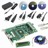
KIT DEV ARRIA II GX FPGA 2AGX125
Manufacturer
Altera
Series
Arria II GXr
Type
FPGAr
Datasheets
1.EP2AGX45CU17C6N.pdf
(96 pages)
2.DK-DEV-2AGX125N.pdf
(48 pages)
3.DK-DEV-2AGX125N.pdf
(64 pages)
Specifications of DK-DEV-2AGX125N
Contents
Board, Cables, CD, DVD, Power Supply
Silicon Manufacturer
Altera
Core Architecture
FPGA
Core Sub-architecture
Arria
Silicon Core Number
EP2
Silicon Family Name
Arria II GX
Rohs Compliant
Yes
For Use With/related Products
EP2AGX125EF35
Lead Free Status / RoHS Status
Lead free / RoHS Compliant
Other names
544-2600
Available stocks
Company
Part Number
Manufacturer
Quantity
Price
Company:

Part Number:
DK-DEV-2AGX125N
Manufacturer:
Altera
Quantity:
135


1–6
Table 1–5. Recommended Operating Conditions for Arria II GX Devices (Part 2 of 2)
Table 1–6. Recommended Operating Conditions for Arria II GZ Devices (Part 1 of 2)
Arria II Device Handbook Volume 3: Device Datasheet and Addendum
t
Notes to
(1) For more information about supply pin connections, refer to the
(2) Altera recommends a 3.0-V nominal battery voltage when connecting V
(3) V
(4) V
V
V
V
V
V
V
V
V
V
V
V
V
V
V
V
V
V
V
V
Symbol
RAMP
CC
CCCB
CCAUX
CCPD
CCIO
CCPGM
CCA_PLL
CCD_PLL
CC_CLKIN
CCBAT
I
O
CCA_L
CCA_R
CCHIP_L
CCR_L
CCR_R
CCT_L
CCT_R
Symbol
security key, you may connect the V
CCPD
CCIO
(2)
(1)
Table
for 3C and 8C I/O banks where the configuration pins reside only supports 3.3-, 3.0-, 2.5-, or 1.8-V voltage levels.
must be 2.5-V for I/O banks with 2.5-V and lower V
Power Supply Ramp time
1–5:
Core voltage and periphery circuitry power
supply
Supplies power for the configuration RAM
bits
Auxiliary supply
I/O pre-driver (3.0 V) power supply
I/O pre-driver (2.5 V) power supply
I/O buffers (3.0 V) power supply
I/O buffers (2.5 V) power supply
I/O buffers (1.8 V) power supply
I/O buffers (1.5 V) power supply
I/O buffers (1.2 V) power supply
Configuration pins (3.0 V) power supply
Configuration pins (2.5 V) power supply
Configuration pins (1.8 V) power supply
PLL analog voltage regulator power supply
PLL digital voltage regulator power supply
Differential clock input power supply
Battery back-up power supply (For design
security volatile key register)
DC input voltage
Output voltage
Transceiver high voltage power (left side)
Transceiver high voltage power (right side)
Transceiver HIP digital power (left side)
Receiver power (left side)
Receiver power (right side)
Transmitter power (left side)
Transmitter power (right side)
Table 1–6
Description
Description
CCBAT
lists the recommended operating conditions for Arria II GZ devices.
to either GND or a 3.0-V power supply.
CCIO
, 3.0-V for 3.0-V V
Normal POR
Arria II Device Family Pin Connection
Condition
Fast POR
Condition
CCBAT
—
—
—
—
—
—
—
—
—
—
—
—
—
—
—
—
—
—
—
—
—
—
—
—
—
—
to a battery for volatile key backup. If you do not use the volatile
CCIO
, and 3.3-V for 3.3-V V
Minimum
2.85/2.375
0.05
0.05
Minimum
2.375
2.375
2.375
1.425
2.375
2.375
2.375
0.87
1.45
2.85
2.85
1.71
1.14
2.85
1.71
0.87
–0.5
0.87
1.05
1.05
1.05
1.05
1.2
Chapter 1: Device Datasheet for Arria II Devices
0
(Note 1)
(Note 6)
Typical
Guidelines.
3.0/2.5
—
—
CCIO
Typical
December 2010 Altera Corporation
0.90
1.50
0.90
2.5
3.0
2.5
3.0
2.5
1.8
1.5
1.2
3.0
2.5
1.8
2.5
2.5
0.9
1.1
1.1
1.1
1.1
—
—
—
.
(4)
Maximum
Electrical Characteristics
100
3.15/2.625
Maximum
4
2.625
2.625
2.625
1.575
2.625
2.625
2.625
V
0.93
1.55
3.15
3.15
1.89
1.26
3.15
1.89
0.93
0.93
1.15
1.15
1.15
1.15
3.3
3.6
CCIO
Unit
ms
ms
Unit
V
V
V
V
V
V
V
V
V
V
V
V
V
V
V
V
V
V
V
V
V
V
V
V
V
Related parts for DK-DEV-2AGX125N
Image
Part Number
Description
Manufacturer
Datasheet
Request
R

Part Number:
Description:
KIT DEV CYCLONE III LS EP3CLS200
Manufacturer:
Altera
Datasheet:

Part Number:
Description:
KIT DEV STRATIX IV FPGA 4SE530
Manufacturer:
Altera
Datasheet:

Part Number:
Description:
KIT DEV FPGA 2AGX260 W/6.375G TX
Manufacturer:
Altera
Datasheet:

Part Number:
Description:
KIT DEV MAX V 5M570Z
Manufacturer:
Altera
Datasheet:

Part Number:
Description:
KIT DEV STRATIX V FPGA 5SGXEA7
Manufacturer:
Altera
Datasheet:

Part Number:
Description:
KIT DEVELOPMENT STRATIX III
Manufacturer:
Altera
Datasheet:

Part Number:
Description:
KIT DEVELOPMENT STRATIX IV
Manufacturer:
Altera
Datasheet:

Part Number:
Description:
KIT DEV ARRIA GX 1AGX60N
Manufacturer:
Altera
Datasheet:
Part Number:
Description:
KIT STARTER CYCLONE IV GX
Manufacturer:
Altera
Datasheet:
Part Number:
Description:
KIT DEVELOPMENT STRATIX IV
Manufacturer:
Altera
Datasheet:

Part Number:
Description:
CPLD, EP610 Family, ECMOS Process, 300 Gates, 16 Macro Cells, 16 Reg., 16 User I/Os, 5V Supply, 35 Speed Grade, 24DIP
Manufacturer:
Altera Corporation
Datasheet:
Part Number:
Description:
CPLD, EP610 Family, ECMOS Process, 300 Gates, 16 Macro Cells, 16 Reg., 16 User I/Os, 5V Supply, 15 Speed Grade, 24DIP
Manufacturer:
Altera Corporation
Datasheet: