DEMO9S08EL32 Freescale Semiconductor, DEMO9S08EL32 Datasheet - Page 27
DEMO9S08EL32
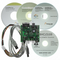
Manufacturer Part Number
DEMO9S08EL32
Description
BOARD DEMO FOR 9S08 EL MCU
Manufacturer
Freescale Semiconductor
Type
MCUr
Datasheets
1.DEMO9S08EL32.pdf
(356 pages)
2.DEMO9S08EL32.pdf
(14 pages)
3.DEMO9S08EL32.pdf
(2 pages)
Specifications of DEMO9S08EL32
Contents
Evaluation Board
Processor To Be Evaluated
MC9S08EL32
Data Bus Width
8 bit
Interface Type
RS-232, USB
Operating Supply Voltage
12 V
Silicon Manufacturer
Freescale
Core Architecture
HCS08
Core Sub-architecture
HCS08
Silicon Core Number
MC9S08
Silicon Family Name
S08EL
Rohs Compliant
Yes
For Use With/related Products
MC9S08EL32
Lead Free Status / RoHS Status
Lead free / RoHS Compliant


2.2.2
Immediately after reset, the MCU uses an internally generated clock provided by the clock source
generator (ICS) module. This internal clock source is used during reset startup and can be enabled as the
clock source for stop recovery to avoid the need for a long crystal startup delay. For more information on
the ICS, see
The oscillator (XOSC) in this MCU is a Pierce oscillator that can accommodate a crystal or ceramic
resonator. Rather than a crystal or ceramic resonator, an external oscillator can be connected to the EXTAL
input pin.
Refer to
resistors such as carbon composition resistors. Wire-wound resistors, and some metal film resistors, have
too much inductance. C1 and C2 normally should be high-quality ceramic capacitors that are specifically
designed for high-frequency applications.
R
is not generally critical. Typical systems use 1 MΩ to 10 MΩ. Higher values are sensitive to humidity and
lower values reduce gain and (in extreme cases) could prevent startup.
C1 and C2 are typically in the 5-pF to 25-pF range and are chosen to match the requirements of a specific
crystal or resonator. Be sure to take into account printed circuit board (PCB) capacitance and MCU pin
capacitance when selecting C1 and C2. The crystal manufacturer typically specifies a load capacitance
which is the series combination of C1 and C2 (which are usually the same size). As a first-order
approximation, use 10 pF as an estimate of combined pin and PCB capacitance for each oscillator pin
(EXTAL and XTAL).
2.2.3
RESET is a dedicated pin with a built in pull-up device. It has input hysteresis and an open drain output.
Since the pin does not have a clamp diode to V
reset and low-voltage reset circuitry typically make external reset circuitry unnecessary. This pin is
normally connected to the standard 6-pin background debug connector so a development system can
directly reset the MCU system. If desired, a manual external reset can be added by supplying a simple
switch to ground (pull reset pin low to force a reset).
Whenever any reset is initiated (whether from an external signal or from an internal system), the RESET
pin is driven low for about 66 bus cycles. The reset circuitry decodes the cause of reset and records it by
setting a corresponding bit in the system reset status register (SRS).
Freescale Semiconductor
F
is used to provide a bias path to keep the EXTAL input in its linear range during crystal startup; its value
Figure 2-3
Oscillator
RESET
Chapter 8, “Internal Clock Source
This pin does not contain a clamp diode to V
above V
is not pulled to V
V
pullup.
DD
. If the RESET pin is required to drive to a V
for the following discussion. R
DD
MC9S08EL32 Series and MC9S08SL16 Series Data Sheet, Rev. 3
. The voltage measured on the internally-pulled-up RESET pin
DD
. The internal gates connected to this pin are pulled to
DD
(S08ICSV2).”
NOTE
, it should not be driven above V
S
(when used) and R
DD
and should not be driven
DD
level, use an external
F
should be low-inductance
Chapter 2 Pins and Connections
DD
. Internal power-on
27
Related parts for DEMO9S08EL32
Image
Part Number
Description
Manufacturer
Datasheet
Request
R

Part Number:
Description:
Manufacturer:
Freescale Semiconductor, Inc
Datasheet:
Part Number:
Description:
Manufacturer:
Freescale Semiconductor, Inc
Datasheet:
Part Number:
Description:
Manufacturer:
Freescale Semiconductor, Inc
Datasheet:
Part Number:
Description:
Manufacturer:
Freescale Semiconductor, Inc
Datasheet:
Part Number:
Description:
Manufacturer:
Freescale Semiconductor, Inc
Datasheet:
Part Number:
Description:
Manufacturer:
Freescale Semiconductor, Inc
Datasheet:
Part Number:
Description:
Manufacturer:
Freescale Semiconductor, Inc
Datasheet:
Part Number:
Description:
Manufacturer:
Freescale Semiconductor, Inc
Datasheet:
Part Number:
Description:
Manufacturer:
Freescale Semiconductor, Inc
Datasheet:
Part Number:
Description:
Manufacturer:
Freescale Semiconductor, Inc
Datasheet:
Part Number:
Description:
Manufacturer:
Freescale Semiconductor, Inc
Datasheet:
Part Number:
Description:
Manufacturer:
Freescale Semiconductor, Inc
Datasheet:
Part Number:
Description:
Manufacturer:
Freescale Semiconductor, Inc
Datasheet:
Part Number:
Description:
Manufacturer:
Freescale Semiconductor, Inc
Datasheet:
Part Number:
Description:
Manufacturer:
Freescale Semiconductor, Inc
Datasheet: