DEMO9S08EL32 Freescale Semiconductor, DEMO9S08EL32 Datasheet - Page 205
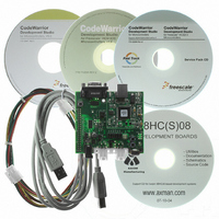
DEMO9S08EL32
Manufacturer Part Number
DEMO9S08EL32
Description
BOARD DEMO FOR 9S08 EL MCU
Manufacturer
Freescale Semiconductor
Type
MCUr
Datasheets
1.DEMO9S08EL32.pdf
(356 pages)
2.DEMO9S08EL32.pdf
(14 pages)
3.DEMO9S08EL32.pdf
(2 pages)
Specifications of DEMO9S08EL32
Contents
Evaluation Board
Processor To Be Evaluated
MC9S08EL32
Data Bus Width
8 bit
Interface Type
RS-232, USB
Operating Supply Voltage
12 V
Silicon Manufacturer
Freescale
Core Architecture
HCS08
Core Sub-architecture
HCS08
Silicon Core Number
MC9S08
Silicon Family Name
S08EL
Rohs Compliant
Yes
For Use With/related Products
MC9S08EL32
Lead Free Status / RoHS Status
Lead free / RoHS Compliant


The SLIC clock is the same as the CPU bus clock. The module is designed to provide better than 1% bit
rate accuracy at the lowest value of the SLIC clock frequency and the accuracy improves as the SLIC clock
frequency is increased. For this reason, it is advantageous to choose the fastest SLIC clock which is still
within the acceptable operating range of the SLIC.Because the SLIC may be used with MCUs with internal
oscillators, the tolerance of the oscillator must be taken into account to ensure that SLIC clock frequency
does not exceed the bounds of the SLIC clock operating range. This is especially important if the user
wishes to use the oscillator untrimmed, where process variations might result in MCU frequency offsets
of ±25%.
The acceptable range of SLIC clock frequencies is 2 to 20 MHz to guarantee LIN operations with greater
than 1.5% accuracy across the 1–20 kbps range of LIN bit rates. The user must ensure that the fastest
possible SLIC clock frequency never exceeds 20 MHz or that the slowest possible SLIC clock never falls
below 2 MHz under worst case conditions. This would include, for example, oscillator frequency
variations due to untrimmed oscillator tolerance, temperature variation, or supply voltage variation.
To initialize the SLIC module into LIN operating mode, the user must perform the following steps prior
to needing to receive any LIN message traffic. These steps assume the MCU has been reset either by a
power-on reset (POR) or any other MCU reset mechanism.
The steps for SLIC Initialization for LIN operation are:
12.6.6.2
Bit rate synchronization is handled automatically in LIN mode, using the synchronization data contained
in each LIN message to derive the desired bit rate. In byte transfer mode (BTM = 1); however, the user
must set up the bit rate for communications using SLCBT.
More information on byte transfer mode is described in
including the performance parameters on recommended maximum speeds, bit time resolution, and
oscillator tolerance requirements.
After the desired settings of bit time are determined, the SLIC Initialization for BTM operation is virtually
identical to that of LIN operation.
The steps are:
Freescale Semiconductor
1. Write SLCC1 to clear INITREQ.
2. When INITACK = 0, write SLCC1 & SLCC2 with desired values for:
3. Write SLCC2 to set up prescalers for:
4. Enable the SLIC module by writing SLCC2:
5. Write SLCC1 to enable SLIC interrupts (if desired).
1. Write SLCC1 to clear INITREQ.
a) SLCWCM — Wait clock mode.
a) RXFP — Digital receive filter clock prescaler.
a) SLCE = 1 to place SLIC module into run mode.
b) BTM = 0 to disable byte transfer mode.
Byte Transfer Mode Initialization
MC9S08EL32 Series and MC9S08SL16 Series Data Sheet, Rev. 3
Section 12.6.16, “Byte Transfer Mode
Operation,”
207
Related parts for DEMO9S08EL32
Image
Part Number
Description
Manufacturer
Datasheet
Request
R

Part Number:
Description:
Manufacturer:
Freescale Semiconductor, Inc
Datasheet:
Part Number:
Description:
Manufacturer:
Freescale Semiconductor, Inc
Datasheet:
Part Number:
Description:
Manufacturer:
Freescale Semiconductor, Inc
Datasheet:
Part Number:
Description:
Manufacturer:
Freescale Semiconductor, Inc
Datasheet:
Part Number:
Description:
Manufacturer:
Freescale Semiconductor, Inc
Datasheet:
Part Number:
Description:
Manufacturer:
Freescale Semiconductor, Inc
Datasheet:
Part Number:
Description:
Manufacturer:
Freescale Semiconductor, Inc
Datasheet:
Part Number:
Description:
Manufacturer:
Freescale Semiconductor, Inc
Datasheet:
Part Number:
Description:
Manufacturer:
Freescale Semiconductor, Inc
Datasheet:
Part Number:
Description:
Manufacturer:
Freescale Semiconductor, Inc
Datasheet:
Part Number:
Description:
Manufacturer:
Freescale Semiconductor, Inc
Datasheet:
Part Number:
Description:
Manufacturer:
Freescale Semiconductor, Inc
Datasheet:
Part Number:
Description:
Manufacturer:
Freescale Semiconductor, Inc
Datasheet:
Part Number:
Description:
Manufacturer:
Freescale Semiconductor, Inc
Datasheet:
Part Number:
Description:
Manufacturer:
Freescale Semiconductor, Inc
Datasheet: