MCP6V01DM-VOS Microchip Technology, MCP6V01DM-VOS Datasheet - Page 7
MCP6V01DM-VOS
Manufacturer Part Number
MCP6V01DM-VOS
Description
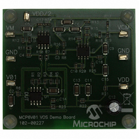
DEMO BOARD FOR MCP6V01
Manufacturer
Microchip Technology
Specifications of MCP6V01DM-VOS
Channels Per Ic
1 - Single
Amplifier Type
Chopper (Zero-Drift)
Output Type
Rail-to-Rail
Slew Rate
0.5 V/µs
Current - Output / Channel
22mA
Operating Temperature
-40°C ~ 125°C
Voltage - Supply, Single/dual (±)
1.8 V ~ 5.5 V
Board Type
Fully Populated
Utilized Ic / Part
MCP6V01
Silicon Manufacturer
Microchip
Application Sub Type
Operational Amplifier
Kit Application Type
Amplifier
Silicon Core Number
MCP6V01, MCP6V03, MCP6V06, MCP6V08
Kit Contents
Board
Lead Free Status / RoHS Status
Lead free / RoHS Compliant
-3db Bandwidth
-
Current - Supply (main Ic)
-
Lead Free Status / Rohs Status
Lead free / RoHS Compliant


2.0
Note: Unless otherwise indicated, T
V
2.1
FIGURE 2-1:
FIGURE 2-2:
FIGURE 2-3:
Quadratic Temp Co.
© 2008 Microchip Technology Inc.
L
Note:
= V
22%
20%
18%
16%
14%
12%
10%
22%
20%
18%
16%
14%
12%
10%
8%
6%
4%
2%
0%
8%
6%
4%
2%
0%
DD
20%
18%
16%
14%
12%
10%
8%
6%
4%
2%
0%
TYPICAL PERFORMANCE CURVES
DC Input Precision
/2, R
78 Samples
V
Soldered on PCB
78 Samples
V
Soldered on PCB
DD
DD
The graphs and tables provided following this note are a statistical summary based on a limited number of
samples and are provided for informational purposes only. The performance characteristics listed herein
are not tested or guaranteed. In some graphs or tables, the data presented may be outside the specified
operating range (e.g., outside specified power supply range) and therefore outside the warranted range.
78 Samples
T
V
Soldered on PCB
Input Offset Voltage's Quadratic Temp Co;
= 1.8V and 5.5V
= 1.8V and 5.5V
A
DD
L
= +25°C
Input Offset Voltage Drift; TC
= 1.8V and 5.5V
= 20 kΩ to V
Input Offset Voltage (µV)
Input Offset Voltage.
Input Offset Voltage Drift.
Input Offset Voltage
TC
2
L
(nV/°C
, C
L
= 60 pF, and CS = GND.
2
)
A
= +25°C, V
1
(nV/°C)
DD
= +1.8V to 5.5V, V
FIGURE 2-4:
Power Supply Voltage with V
FIGURE 2-5:
Power Supply Voltage with V
FIGURE 2-6:
Output Voltage.
-1
-2
-3
-4
-1
-2
-3
-4
-1
-2
-3
-4
4
3
2
1
0
4
3
2
1
0
4
3
2
1
0
0.0 0.5 1.0 1.5 2.0 2.5 3.0 3.5 4.0 4.5 5.0 5.5 6.0 6.5
0.0 0.5 1.0 1.5 2.0 2.5 3.0 3.5 4.0 4.5 5.0 5.5 6.0 6.5
0.0 0.5 1.0 1.5 2.0 2.5 3.0 3.5 4.0 4.5 5.0 5.5
SS
= GND, V
V
DD
= 1.8V
Representative Part
Power Supply Voltage (V)
Power Supply Voltage (V)
CM
MCP6V01/2/3
Output Voltage (V)
Input Offset Voltage vs.
Input Offset Voltage vs.
Input Offset Voltage vs.
= V
+125°C
+85°C
+25°C
-40°C
DD
+125°C
+85°C
+25°C
-40°C
/3, V
CM
CM
OUT
V
DD
= V
= V
= 5.5V
V
Representative Part
V
Representative Part
DS22058C-page 7
CM
CM
= V
= V
CMR_L
= V
CMR_H
DD
CMR_L
CMR_H
/2,
.
.
Related parts for MCP6V01DM-VOS
Image
Part Number
Description
Manufacturer
Datasheet
Request
R

Part Number:
Description:
IC OPAMP AUTO-ZERO SNGL 8SOIC
Manufacturer:
Microchip Technology
Datasheet:

Part Number:
Description:
300 ?A, Auto-Zeroed Op Amps
Manufacturer:
MICROCHIP [Microchip Technology]
Datasheet:
Part Number:
Description:
Op Amps Sngl Auto-Zero Op Amp E temp
Manufacturer:
Microchip Technology

Part Number:
Description:
300 ?a, Auto-zeroed Op Amps
Manufacturer:
Microchip Technology Inc.
Datasheet:
Part Number:
Description:
Manufacturer:
Microchip Technology Inc.
Datasheet:
Part Number:
Description:
Manufacturer:
Microchip Technology Inc.
Datasheet:
Part Number:
Description:
Manufacturer:
Microchip Technology Inc.
Datasheet:
Part Number:
Description:
Manufacturer:
Microchip Technology Inc.
Datasheet:
Part Number:
Description:
Manufacturer:
Microchip Technology Inc.
Datasheet:
Part Number:
Description:
Manufacturer:
Microchip Technology Inc.
Datasheet:
Part Number:
Description:
Manufacturer:
Microchip Technology Inc.
Datasheet: