MCP6V01DM-VOS Microchip Technology, MCP6V01DM-VOS Datasheet - Page 19
MCP6V01DM-VOS
Manufacturer Part Number
MCP6V01DM-VOS
Description
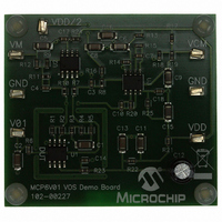
DEMO BOARD FOR MCP6V01
Manufacturer
Microchip Technology
Specifications of MCP6V01DM-VOS
Channels Per Ic
1 - Single
Amplifier Type
Chopper (Zero-Drift)
Output Type
Rail-to-Rail
Slew Rate
0.5 V/µs
Current - Output / Channel
22mA
Operating Temperature
-40°C ~ 125°C
Voltage - Supply, Single/dual (±)
1.8 V ~ 5.5 V
Board Type
Fully Populated
Utilized Ic / Part
MCP6V01
Silicon Manufacturer
Microchip
Application Sub Type
Operational Amplifier
Kit Application Type
Amplifier
Silicon Core Number
MCP6V01, MCP6V03, MCP6V06, MCP6V08
Kit Contents
Board
Lead Free Status / RoHS Status
Lead free / RoHS Compliant
-3db Bandwidth
-
Current - Supply (main Ic)
-
Lead Free Status / Rohs Status
Lead free / RoHS Compliant


3.0
Descriptions of the pins are listed in
TABLE 3-1:
3.1
The analog output pins (V
voltage sources.
3.2
The non-inverting and inverting inputs (V
are high-impedance CMOS inputs with low bias
currents.
3.3
The positive power supply (V
than the negative power supply (V
operation, the other pins are between V
Typically, these parts are used in a single (positive)
supply configuration. In this case, V
ground and V
need bypass capacitors.
© 2008 Microchip Technology Inc.
1, 5, 8
TDFN
—
—
—
—
6
2
3
4
7
9
MCP6V01
PIN DESCRIPTIONS
Analog Outputs
Analog Inputs
Power Supply Pins
1, 5, 8
DD
SOIC
—
—
—
—
—
6
2
3
4
7
is connected to the supply. V
PIN FUNCTION TABLE
DFN
—
—
1
2
3
4
5
6
7
8
9
OUT
DD
MCP6V02
) is 1.8V to 5.5V higher
) are low-impedance
SS
Table
SOIC
SS
is connected to
—
—
—
SS
1
2
3
4
5
6
7
8
). For normal
IN
3-1.
and V
+, V
IN
DD
DD
1, 5, 8
–, …)
TDFN
—
—
—
—
6
2
3
4
7
9
.
will
MCP6V03
SOIC
1, 5
—
—
—
—
6
2
3
4
7
8
3.4
This pin (CS) is a CMOS, Schmitt-triggered input that
places the MCP6V03 op amps into a low power mode
of operation.
3.5
There is an internal connection between the Exposed
Thermal Pad (EP) and the V
nected to the same potential on the Printed Circuit
Board (PCB).
This pad can be connected to a PCB ground plane to
provide a larger heat sink. This improves the package
thermal resistance (
V
Chip Select (CS) Digital Input
Exposed Thermal Pad (EP)
V
V
OUT
IN
IN
Symbol
V
V
V
–, V
+, V
V
V
OUTB
CS
NC
INB
EP
, V
INB
DD
SS
OUTA
INA
INA
+
–
–
+
MCP6V01/2/3
θ
JA
).
Output (op amp A)
Inverting Input (op amp A)
Non-inverting Input
(op amp A)
Negative Power Supply
Non-inverting Input
(op amp B)
Inverting Input (op amp B)
Output (op amp B)
Positive Power Supply
Chip Select (op amp A)
No Internal Connection
Exposed Thermal Pad (EP);
must be connected to V
SS
pin; they must be con-
Description
DS22058C-page 19
SS
Related parts for MCP6V01DM-VOS
Image
Part Number
Description
Manufacturer
Datasheet
Request
R

Part Number:
Description:
IC OPAMP AUTO-ZERO SNGL 8SOIC
Manufacturer:
Microchip Technology
Datasheet:

Part Number:
Description:
300 ?A, Auto-Zeroed Op Amps
Manufacturer:
MICROCHIP [Microchip Technology]
Datasheet:
Part Number:
Description:
Op Amps Sngl Auto-Zero Op Amp E temp
Manufacturer:
Microchip Technology

Part Number:
Description:
300 ?a, Auto-zeroed Op Amps
Manufacturer:
Microchip Technology Inc.
Datasheet:
Part Number:
Description:
Manufacturer:
Microchip Technology Inc.
Datasheet:
Part Number:
Description:
Manufacturer:
Microchip Technology Inc.
Datasheet:
Part Number:
Description:
Manufacturer:
Microchip Technology Inc.
Datasheet:
Part Number:
Description:
Manufacturer:
Microchip Technology Inc.
Datasheet:
Part Number:
Description:
Manufacturer:
Microchip Technology Inc.
Datasheet:
Part Number:
Description:
Manufacturer:
Microchip Technology Inc.
Datasheet:
Part Number:
Description:
Manufacturer:
Microchip Technology Inc.
Datasheet: