MCP6V01DM-VOS Microchip Technology, MCP6V01DM-VOS Datasheet - Page 23
MCP6V01DM-VOS
Manufacturer Part Number
MCP6V01DM-VOS
Description
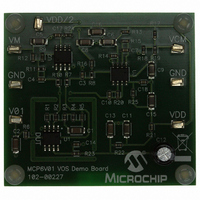
DEMO BOARD FOR MCP6V01
Manufacturer
Microchip Technology
Specifications of MCP6V01DM-VOS
Channels Per Ic
1 - Single
Amplifier Type
Chopper (Zero-Drift)
Output Type
Rail-to-Rail
Slew Rate
0.5 V/µs
Current - Output / Channel
22mA
Operating Temperature
-40°C ~ 125°C
Voltage - Supply, Single/dual (±)
1.8 V ~ 5.5 V
Board Type
Fully Populated
Utilized Ic / Part
MCP6V01
Silicon Manufacturer
Microchip
Application Sub Type
Operational Amplifier
Kit Application Type
Amplifier
Silicon Core Number
MCP6V01, MCP6V03, MCP6V06, MCP6V08
Kit Contents
Board
Lead Free Status / RoHS Status
Lead free / RoHS Compliant
-3db Bandwidth
-
Current - Supply (main Ic)
-
Lead Free Status / Rohs Status
Lead free / RoHS Compliant


4.2
4.2.1
The input stage of the MCP6V01/2/3 op amps uses two
differential CMOS input stages in parallel. One
operates at low common mode input voltage (V
which is approximately equal to V
mal operation) and the other at high V
topology, the input operates with V
either supply rail at +25°C (see
offset voltage (V
and V
The transition between the input stages occurs when
V
the best distortion and gain linearity, with non-inverting
gains, avoid this region of operation.
4.2.1.1
The input devices are designed to not exhibit phase
inversion when the input pins exceed the supply
voltages.
exceeding both supplies with no phase inversion.
4.2.1.2
The ESD protection on the inputs can be depicted as
shown in
protect the input transistors, and to minimize input bias
current (I
when they try to go more than one diode drop below
V
above V
allow normal operation, and low enough to bypass
quick ESD events within the specified limits.
FIGURE 4-4:
Structures.
In order to prevent damage and/or improper operation
of these amplifiers, the circuit must limit the currents
(and voltages) at the input pins (see Section 1.1
“Absolute Maximum Ratings †”).
the recommended approach to protecting these inputs.
The internal ESD diodes prevent the input pins (V
and V
resistors R
of the input pins. Diodes D
© 2008 Microchip Technology Inc.
CM
SS
. They also clamp any voltages that go too far
V
≈ V
V
V
DD
IN
IN
DD
SS
–) from going too far below ground, and the
+
DD
DD
Other Functional Blocks
+ 0.2V to ensure proper operation.
B
). The input ESD diodes clamp the inputs
Figure
1
; their breakdown voltage is high enough to
– 0.9V (see
Figure 2-43
Bond
Bond
Bond
RAIL-TO-RAIL INPUTS
Pad
Pad
Pad
and R
Phase Reversal
Input Voltage and Current Limits
OS
4-4. This structure was chosen to
2
) is measured at V
limit the possible current drawn out
Simplified Analog Input ESD
Figure 2-7
Stage
Input
shows
1
and D
Figure
IN
and
an
CM
2
+ and V
Figure 4-5
prevent the input
Bond
CM
Pad
2-18). The input
up to 0.2V past
Figure
input
CM
= V
. With this
IN
SS
V
– in nor-
2-8). For
IN
voltage
– 0.2V
shows
–
CM
IN
+
,
pins (V
dump any currents onto V
shown, resistors R
through D
FIGURE 4-5:
Inputs.
It is also possible to connect the diodes to the left of the
resistor R
the diodes D
mechanism. The resistors then serve as in-rush current
limiters; the DC current into the input pins (V
V
A significant amount of current can flow out of the
inputs (through the ESD diodes) when the common
mode voltage (V
Figure
need to limit the usable voltage range.
4.2.2
The output voltage range of the MCP6V01/2/3
auto-zeroed op amps is V
V
connected to V
Figure 2-19
These op amps are designed to drive light loads; use
another amplifier to buffer the output from heavy loads.
4.2.3
The single MCP6V03 has a Chip Select (CS) pin.
When CS is pulled high, the supply current for the
corresponding op amp drops to about 1 µA (typical),
and is pulled through the CS pin to V
happens, the amplifier is put into a high impedance
state. By pulling CS low, the amplifier is enabled. If the
CS pin is left floating, the internal pull-down resistor
(about 5 MΩ) will keep the part on.
the output voltage and supply current response to a CS
pulse.
IN
SS
–) should be very small.
+ 15 mV
V
V
1
2
IN
2-17. Applications that are high impedance may
+ and V
R
R
1
1
1
2
and D
and R
RAIL-TO-RAIL OUTPUT
CHIP SELECT (CS)
and
1
R
R
>
>
and D
D
1
2
V
V
(maximum)
1
SS
SS
IN
Figure 2-20
2
2
–) from going too far above V
D
DD
CM
.
. In this case, the currents through
– (minimum expected V
– (minimum expected V
MCP6V01/2/3
2
1
2
/2 and V
) is below ground (V
need to be limited by some other
and R
Protecting the Analog
MCP6V0X
DD
DD
2 mA
2 mA
for more information.
2
. When implemented as
– 15 mV (minimum) and
V
when
also limit the current
DD
DD
= 5.5V. Refer to
DS22058C-page 23
Figure 1-4
R
SS
L
= 20 kΩ
. When this
1
2
)
)
V
SS
OUT
IN
DD
); see
shows
+ and
, and
is
Related parts for MCP6V01DM-VOS
Image
Part Number
Description
Manufacturer
Datasheet
Request
R

Part Number:
Description:
IC OPAMP AUTO-ZERO SNGL 8SOIC
Manufacturer:
Microchip Technology
Datasheet:

Part Number:
Description:
300 ?A, Auto-Zeroed Op Amps
Manufacturer:
MICROCHIP [Microchip Technology]
Datasheet:
Part Number:
Description:
Op Amps Sngl Auto-Zero Op Amp E temp
Manufacturer:
Microchip Technology

Part Number:
Description:
300 ?a, Auto-zeroed Op Amps
Manufacturer:
Microchip Technology Inc.
Datasheet:
Part Number:
Description:
Manufacturer:
Microchip Technology Inc.
Datasheet:
Part Number:
Description:
Manufacturer:
Microchip Technology Inc.
Datasheet:
Part Number:
Description:
Manufacturer:
Microchip Technology Inc.
Datasheet:
Part Number:
Description:
Manufacturer:
Microchip Technology Inc.
Datasheet:
Part Number:
Description:
Manufacturer:
Microchip Technology Inc.
Datasheet:
Part Number:
Description:
Manufacturer:
Microchip Technology Inc.
Datasheet:
Part Number:
Description:
Manufacturer:
Microchip Technology Inc.
Datasheet: