MCP6V01DM-VOS Microchip Technology, MCP6V01DM-VOS Datasheet - Page 27
MCP6V01DM-VOS
Manufacturer Part Number
MCP6V01DM-VOS
Description
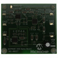
DEMO BOARD FOR MCP6V01
Manufacturer
Microchip Technology
Specifications of MCP6V01DM-VOS
Channels Per Ic
1 - Single
Amplifier Type
Chopper (Zero-Drift)
Output Type
Rail-to-Rail
Slew Rate
0.5 V/µs
Current - Output / Channel
22mA
Operating Temperature
-40°C ~ 125°C
Voltage - Supply, Single/dual (±)
1.8 V ~ 5.5 V
Board Type
Fully Populated
Utilized Ic / Part
MCP6V01
Silicon Manufacturer
Microchip
Application Sub Type
Operational Amplifier
Kit Application Type
Amplifier
Silicon Core Number
MCP6V01, MCP6V03, MCP6V06, MCP6V08
Kit Contents
Board
Lead Free Status / RoHS Status
Lead free / RoHS Compliant
-3db Bandwidth
-
Current - Supply (main Ic)
-
Lead Free Status / Rohs Status
Lead free / RoHS Compliant


4.3.9.3
Figure 4-12
fier circuit. Usually, we choose R
The guard traces (with ground vias at the ends) help
minimize the thermal gradients. The resistor layout
cancels the resistor thermal voltages, assuming the
temperature gradient is constant near the resistors:
EQUATION 4-3:
FIGURE 4-12:
for Single Difference Amplifier.
© 2008 Microchip Technology Inc.
Where:
Thermal voltages are approximately equal
Note:
V
G
V
M
P
DM
V
V
M
P
Changing the orientation of the resistors
will usually cause a significant decrease in
the cancellation of the thermal voltages.
shows the recommended difference ampli-
V
V
=
MCP6V01
Difference Amplifier Layout for
Thermo-junctions
OUT
OUT
R4
R2
R1
R3
R
V
R
≈ V
≈ V
R
3
OS
1
2
/R
U
REF
REF
is neglected
1
1
PCB Layout and Schematic
= R
+ (V
+ (V
4
R
R
/R
P
P
4
3
U1
2
– V
– V
, difference gain
1
= R
M
M
V
)G
)G
2
REF
DM
DM
V
and R
OUT
V
V
3
OUT
REF
= R
4
.
4.3.9.4
The dual op amp amplifiers shown in
Figure 4-17
greater than 1, and a common mode gain of 1 .They
can use the layout shown in
ting resistors (R
bined so that the thermal voltages can be canceled.
The guard traces (with ground vias at the ends) help
minimize the thermal gradients. The resistor layout
cancels the resistor thermal voltages, assuming the
temperature gradient is constant near the resistors:
EQUATION 4-4:
FIGURE 4-13:
for Dual Non-inverting Amplifier.
Where:
Thermal voltages are approximately equal
Note:
G
G
R3
R2
R1
DM
CM
V
V
IA
IB
=
=
Changing the orientation of the resistors
will usually cause a significant decrease in
the cancellation of the thermal voltages.
(V
(V
produce a non-inverting difference gain
Dual Non-inverting Amplifier Layout
for Thermo-junctions
½ MCP6V02
½ MCP6V02
OA
OA
1 + R
1, common mode gain
V
2
) between the two sides are not com-
OS
– V
+ V
V
MCP6V01/2/3
is neglected
3
OB
OA
OB
R
R
R
R
/R
V
PCB Layout and Schematic
1
1
2
2
IA
U1
) ≈ (V
)/2 ≈ (V
2
U
U
, differential mode gain
1
1
V
Figure
IA
IB
IA
– V
R
R
V
3
3
+ V
OB
IB
4-13. The gain set-
DS22058C-page 27
)G
IB
Figure 4-16
)/2
DM
V
V
OA
OB
R3
R2
R1
and
Related parts for MCP6V01DM-VOS
Image
Part Number
Description
Manufacturer
Datasheet
Request
R

Part Number:
Description:
IC OPAMP AUTO-ZERO SNGL 8SOIC
Manufacturer:
Microchip Technology
Datasheet:

Part Number:
Description:
300 ?A, Auto-Zeroed Op Amps
Manufacturer:
MICROCHIP [Microchip Technology]
Datasheet:
Part Number:
Description:
Op Amps Sngl Auto-Zero Op Amp E temp
Manufacturer:
Microchip Technology

Part Number:
Description:
300 ?a, Auto-zeroed Op Amps
Manufacturer:
Microchip Technology Inc.
Datasheet:
Part Number:
Description:
Manufacturer:
Microchip Technology Inc.
Datasheet:
Part Number:
Description:
Manufacturer:
Microchip Technology Inc.
Datasheet:
Part Number:
Description:
Manufacturer:
Microchip Technology Inc.
Datasheet:
Part Number:
Description:
Manufacturer:
Microchip Technology Inc.
Datasheet:
Part Number:
Description:
Manufacturer:
Microchip Technology Inc.
Datasheet:
Part Number:
Description:
Manufacturer:
Microchip Technology Inc.
Datasheet:
Part Number:
Description:
Manufacturer:
Microchip Technology Inc.
Datasheet: