MCP6V01DM-VOS Microchip Technology, MCP6V01DM-VOS Datasheet - Page 6
MCP6V01DM-VOS
Manufacturer Part Number
MCP6V01DM-VOS
Description
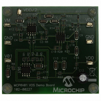
DEMO BOARD FOR MCP6V01
Manufacturer
Microchip Technology
Specifications of MCP6V01DM-VOS
Channels Per Ic
1 - Single
Amplifier Type
Chopper (Zero-Drift)
Output Type
Rail-to-Rail
Slew Rate
0.5 V/µs
Current - Output / Channel
22mA
Operating Temperature
-40°C ~ 125°C
Voltage - Supply, Single/dual (±)
1.8 V ~ 5.5 V
Board Type
Fully Populated
Utilized Ic / Part
MCP6V01
Silicon Manufacturer
Microchip
Application Sub Type
Operational Amplifier
Kit Application Type
Amplifier
Silicon Core Number
MCP6V01, MCP6V03, MCP6V06, MCP6V08
Kit Contents
Board
Lead Free Status / RoHS Status
Lead free / RoHS Compliant
-3db Bandwidth
-
Current - Supply (main Ic)
-
Lead Free Status / Rohs Status
Lead free / RoHS Compliant


MCP6V01/2/3
1.3
FIGURE 1-1:
FIGURE 1-2:
Time.
FIGURE 1-3:
FIGURE 1-4:
DS22058C-page 6
V
V
OUT
V
V
V
I
CS
I
I
V
OUT
DD
SS
CS
V
OS
DD
OS
IN
IN
1 µA
(typical)
-2 µA
(typical)
V
(typical)
Timing Diagrams
V
0V
DD
DD
High-Z
/5 MΩ
t
t
ODR
ON
1.8V
t
V
t
STL
STR
IL
Amplifier Start Up.
Offset Correction Settling
Output Overdrive Recovery.
Chip Select (MCP6V03).
V
DD
(typical)
(typical)
(typical)
300 µA
300 µA
/2
5 pA
V
SS
V
t
ODR
IH
1.8V to 5.5V
V
V
V
V
OS
OS
OS
OS
t
OFF
V
+ 50 µV
– 50 µV
+ 50 µV
+ 50 µV
DD
(typical)
(typical)
(typical)
High-Z
/5 MΩ
-2 µA
1 µA
1.4
The circuits used for the DC and AC tests are shown in
Figure 1-5
out as discussed in Section 4.3.8 “Supply Bypassing
and Filtering”. R
of R
FIGURE 1-5:
Most Non-Inverting Gain Conditions.
FIGURE 1-6:
Most Inverting Gain Conditions.
The circuit in
dynamic behavior (i.e., IMD, t
potentiometer balances the resistor network (V
should equal V
mode input voltage is V
input (V
10 V/V.
FIGURE 1-7:
Input Behavior.
V
V
V
V
V
DD
DD
IN
F
IN
IN
MCP6V0X
MCP6V0X
and R
/3
/3
20.0 kΩ
20.0 kΩ
ERR
0.1%
0.1%
Test Circuits
R
R
R
R
N
G
N
G
and
G
) appears at V
to minimize bias current effects.
Figure
Figure 1-7
REF
20.0 kΩ
MCP6V0X
20.0 kΩ
N
0.1%
0.1%
V
V
V
DD
DD
DD
is equal to the parallel combination
at DC). The op amp’s common
AC and DC Test Circuit for
AC and DC Test Circuit for
Test Circuit for Dynamic
100 nF
100 nF
100 nF
1-6. Lay the bypass capacitors
1 µF
© 2008 Microchip Technology Inc.
CM
R
R
25 turn
24.9 Ω
1 µF
1 µF
50Ω
F
F
tests the op amp input’s
OUT
= V
STR
IN
R
R
with a noise gain of
, t
/2. The error at the
ISO
ISO
R
STL
C
C
ISO
L
L
C
and t
L
V
REF
R
R
L
L
ODR
V
V
V
L
L
L
V
V
V
R
). The
OUT
OUT
OUT
L
OUT
Related parts for MCP6V01DM-VOS
Image
Part Number
Description
Manufacturer
Datasheet
Request
R

Part Number:
Description:
IC OPAMP AUTO-ZERO SNGL 8SOIC
Manufacturer:
Microchip Technology
Datasheet:

Part Number:
Description:
300 ?A, Auto-Zeroed Op Amps
Manufacturer:
MICROCHIP [Microchip Technology]
Datasheet:
Part Number:
Description:
Op Amps Sngl Auto-Zero Op Amp E temp
Manufacturer:
Microchip Technology

Part Number:
Description:
300 ?a, Auto-zeroed Op Amps
Manufacturer:
Microchip Technology Inc.
Datasheet:
Part Number:
Description:
Manufacturer:
Microchip Technology Inc.
Datasheet:
Part Number:
Description:
Manufacturer:
Microchip Technology Inc.
Datasheet:
Part Number:
Description:
Manufacturer:
Microchip Technology Inc.
Datasheet:
Part Number:
Description:
Manufacturer:
Microchip Technology Inc.
Datasheet:
Part Number:
Description:
Manufacturer:
Microchip Technology Inc.
Datasheet:
Part Number:
Description:
Manufacturer:
Microchip Technology Inc.
Datasheet:
Part Number:
Description:
Manufacturer:
Microchip Technology Inc.
Datasheet: