MCP6V01DM-VOS Microchip Technology, MCP6V01DM-VOS Datasheet
MCP6V01DM-VOS
Specifications of MCP6V01DM-VOS


Related parts for MCP6V01DM-VOS


MCP6V01DM-VOS Summary of contents
Page 1
... Microchip Technology Inc. MCP6V01 Input Offset Demo Board User’s Guide DS51801A ...
Page 2
... PowerMate, PowerTool, REAL ICE, rfLAB, Select Mode, Total Endurance, WiperLock and ZENA are trademarks of Microchip Technology Incorporated in the U.S.A. and other countries. SQTP is a service mark of Microchip Technology Incorporated in the U.S.A. All other trademarks mentioned herein are property of their respective companies. ...
Page 3
... A.4 Top Silk Screen A.5 Top Metal Layer A.6 Bottom Metal Layer Appendix B. Bill Of Materials (BOM) B.1 MCP6V01 Input Offset Demo Board BOM ................................................... 19 Worldwide Sales and Service .................................................................................... 20 © 2009 Microchip Technology Inc. MCP6V01 INPUT OFFSET DEMO BOARD USER’S GUIDE Table of Contents ........................................................................................ 17 ....................................................................................... 18 ...
Page 4
... MCP6V01 Input Offset Demo Board User’s Guide NOTES: DS51801A-page iv © 2009 Microchip Technology Inc. ...
Page 5
... MCP6V01 Input Offset Demo Board. • Appendix B. “Bill Of Materials (BOM)” – Lists the parts used to build the sub-assemblies in the MCP6V01 Input Offset Demo Board. © 2009 Microchip Technology Inc. MCP6V01 INPUT OFFSET DEMO BOARD USER’S GUIDE ...
Page 6
... Optional arguments mcc18 [options] file [options] Choice of mutually exclusive errorlevel {0|1} arguments selection Replaces repeated text var_name [, var_name...] Represents code supplied by void main (void) user { ... } © 2009 Microchip Technology Inc. Examples ® IDE User’s Guide ...
Page 7
... Customers should contact their distributor, representative or field application engineer for support. Local sales offices are also available to help customers. A listing of sales offices and locations is included in the back of this document. Technical support is available through the web site at: http://support.microchip.com © 2009 Microchip Technology Inc. OS Drift over Temperature. OS ...
Page 8
... MCP6V01 Input Offset Demo Board User’s Guide DOCUMENT REVISION HISTORY Revision A (March 2009) • Initial Release of this Document. DS51801A-page 4 © 2009 Microchip Technology Inc. ...
Page 9
... Chapter 1. Product Overview 1.1 INTRODUCTION The MCP6V01 Input Offset Demo Board is described by the following: • Assembly # : 102-00227-R3 • Order # : MCP6V01DM-VOS • Name: MCP6V01 Input Offset Demo Board Items discussed in this chapter include: • Kit Contents • Intended Use • Description 1.2 ...
Page 10
... V and GND set the conditions for the DUT driven by an external voltage source, the resistor divider has no CM ≈ 10.0 kV under a variety of bias OS /Δ Outputs GND V . REF half, then buffers that when that input is left DD © 2009 Microchip Technology Inc. ...
Page 11
... Allow the DUT to be biased at most valid bias points • Allow V to set by the circuit The outputs: • Make it easy to measure the important bias voltages V • Make it easy to measure V © 2009 Microchip Technology Inc. Product Overview ) CM ≈ 10.0 V/V) to the term ...
Page 12
... MCP6V01 Input Offset Demo Board User’s Guide NOTES: DS51801A-page 8 © 2009 Microchip Technology Inc. ...
Page 13
... Voltmeter VM –VDD/2 Voltmeter VDD/2 – GND Voltmeter VO1 – GND FIGURE 2-1: © 2009 Microchip Technology Inc. MCP6V01 INPUT OFFSET DEMO BOARD USER’S GUIDE ) OS Board Connections for the MCP6V01 Input Offset Demo Board. Voltmeter VCM – GND Power Supply VCM – ...
Page 14
... OST 2 ⁄ ) ⋅ ( ⁄ ≈ 10.0 µV/V /Δ – ΔV )/Δ /ΔV OS and other changes in input offset as bias voltages and temperature – 0.3V for proper DD are related to specifications OS ) specification applies to one bias OS ) includes OST © 2009 Microchip Technology Inc. ...
Page 15
... Note OUT Based on these measurements, we can make the following estimates, where the V values are calculated from the measured V OST_k © 2009 Microchip Technology Inc. Installation and Operation changes with the common mode input OST COMMON MODE CHANGE EXAMPLE changed on this demo board, the output forced to change by the same amount ...
Page 16
... A DD – V /2) once a second for 16 seconds ( Estimate Units µV/V – (3.7V) µV/V OST_5 µV µV µV µV – (165°C) µV/°C OST_8 – (4.5V) µV/V OST_3 µV – (1.2V) µV/V OST_6 . referred to the input © 2009 Microchip Technology Inc. ...
Page 17
... Solder a MCP6V06 op amp in its place. Use a MCP6V06 in a SOIC-8 package. Pin 1 is next to the U1 reference designator on the PCB (not next to the DUT label) FIGURE 3-1: © 2009 Microchip Technology Inc. MCP6V01 INPUT OFFSET DEMO BOARD USER’S GUIDE Label Reference Designator DUT’ ...
Page 18
... Solder the other end of the wire the closest ground via on the PCB. The striped green arrow to the right in the figure shows the location. The solid green curve represents the wire. FIGURE 3-2: DS51801A-page 14 DUT’s Pin 8 Ground Via Location and Orientation of DUT. Draft © 2009 Microchip Technology Inc. ...
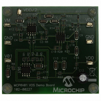
Page 19
... On the top right is the mid-supply reference (V buffer. On the middle right is the common mode voltage reference (VCM) with buffer. On the bottom are the supply bypass capacitors and filter resistors. © 2009 Microchip Technology Inc. MCP6V01 INPUT OFFSET DEMO BOARD USER’S GUIDE ) times a gain ...
Page 20
... MCP6V01 Input Offset Demo Board User’s Guide A.2 BOARD SCHEMATIC (Continued) DS51801A-page 16 © 2009 Microchip Technology Inc. ...
Page 21
... A.3 COMBINATION OF THE TOP SILK SCREEN AND TOP METAL LAYERS A.4 TOP SILK SCREEN © 2009 Microchip Technology Inc. Schematics and Layouts DS51801A-page 17 ...
Page 22
... MCP6V01 Input Offset Demo Board User’s Guide A.5 TOP METAL LAYER A.6 BOTTOM METAL LAYER DS51801A-page 18 © 2009 Microchip Technology Inc. ...
Page 23
... PCB mounting) Stand-off, Hex, 0.500", 4 × 40 Thread, Nylon, 0.285" max. O.D. 4 (for PCB mounting) Machine Screw, Phillips, 4 × 40 Thread, 1/4" long, Nylon © 2009 Microchip Technology Inc. MCP6V01 INPUT OFFSET DEMO BOARD USER’S GUIDE Description Manufacturer Panasonic n/a Susumu Co. Ltd. ...
Page 24
... Fax: 886-3-6578-370 Taiwan - Kaohsiung Tel: 886-7-536-4818 Fax: 886-7-536-4803 Taiwan - Taipei Tel: 886-2-2500-6610 Fax: 886-2-2508-0102 Thailand - Bangkok Tel: 66-2-694-1351 Fax: 66-2-694-1350 © 2009 Microchip Technology Inc. EUROPE Austria - Wels Tel: 43-7242-2244-39 Fax: 43-7242-2244-393 Denmark - Copenhagen Tel: 45-4450-2828 Fax: 45-4485-2829 France - Paris Tel: 33-1-69-53-63-20 ...