MCP6V01DM-VOS Microchip Technology, MCP6V01DM-VOS Datasheet - Page 3
MCP6V01DM-VOS
Manufacturer Part Number
MCP6V01DM-VOS
Description
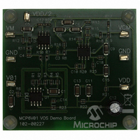
DEMO BOARD FOR MCP6V01
Manufacturer
Microchip Technology
Specifications of MCP6V01DM-VOS
Channels Per Ic
1 - Single
Amplifier Type
Chopper (Zero-Drift)
Output Type
Rail-to-Rail
Slew Rate
0.5 V/µs
Current - Output / Channel
22mA
Operating Temperature
-40°C ~ 125°C
Voltage - Supply, Single/dual (±)
1.8 V ~ 5.5 V
Board Type
Fully Populated
Utilized Ic / Part
MCP6V01
Silicon Manufacturer
Microchip
Application Sub Type
Operational Amplifier
Kit Application Type
Amplifier
Silicon Core Number
MCP6V01, MCP6V03, MCP6V06, MCP6V08
Kit Contents
Board
Lead Free Status / RoHS Status
Lead free / RoHS Compliant
-3db Bandwidth
-
Current - Supply (main Ic)
-
Lead Free Status / Rohs Status
Lead free / RoHS Compliant


1.0
1.1
V
Current at Input Pins ....................................................±2 mA
Analog Inputs (V
All other Inputs and Outputs ............ V
Difference Input voltage ...................................... |V
Output Short Circuit Current ................................ Continuous
Current at Output and Supply Pins ............................±30 mA
Storage Temperature ...................................-65°C to +150°C
Max. Junction Temperature ........................................ +150°C
ESD protection on all pins (HBM, MM) ................≥ 4 kV, 300V
1.2
TABLE 1-1:
© 2008 Microchip Technology Inc.
Electrical Characteristics: Unless otherwise indicated, T
V
Input Offset
Input Offset Voltage
Input Offset Voltage Drift with Temperature
Input Offset Voltage Quadratic Temp. Co.
Power Supply Rejection
Input Bias Current and Impedance
Input Bias Current
Input Bias Current across Temperature
Input Offset Current
Input Offset Current across Temperature
Common Mode Input Impedance
Differential Input Impedance
Common Mode
Common-Mode Input Voltage Range
Common-Mode Rejection
Open-Loop Gain
Note 1:
DD
DC Open-Loop Gain (large signal)
OUT
(linear Temp. Co.)
– V
= V
2:
SS
Absolute Maximum Ratings †
Specifications
DD
.......................................................................6.5V
/2, V
Set by design and characterization. Due to thermal junction and other effects in the production environment, these parts
can only be screened in production (except TC
Figure 2-18
ELECTRICAL CHARACTERISTICS
Parameters
IN
L
+ and V
= V
DC ELECTRICAL SPECIFICATIONS
DD
/2, R
shows how V
IN
–) †† ... V
L
= 20 kΩ to V
SS
SS
CMR
– 1.0V to V
– 0.3V to V
changed across temperature for the first three production lots.
L
, and CS = GND (refer to
CMRR
CMRR
PSRR
V
Sym
Z
V
Z
TC
TC
A
A
I
I
I
DIFF
CMR
I
I
I
OS
OS
OS
CM
OS
OL
OL
B
B
B
DD
1
2
DD
DD
– V
+1.0V
+0.3V
SS
V
A
SS
1
|
= +25°C, V
-1000
; see Appendix B: “Offset Related Test Screens”).
Min
-2.0
130
130
140
130
140
-50
—
—
—
—
—
—
—
—
− 0.20
Figure 1-5
10
10
†
Maximum Ratings” may cause permanent damage to the
device. This is a stress rating only and functional operation of
the device at those or any other conditions above those
indicated in the operational listings of this specification is not
implied. Exposure to maximum rating conditions for extended
periods may affect device reliability.
††
DD
Typ
±0.1
143
600
142
152
145
156
-30
-50
-75
—
—
±1
60
—
Notice: Stresses above those listed under “Absolute
13
13
See Section 4.2.1 “Rail-to-Rail Inputs”.
= +1.8V to +5.5V, V
||6
||6
V
DD
and
Max
5000
1000
+2.0
+50
—
—
—
—
—
—
—
—
—
—
—
—
+ 0.20
Figure
1-6).
nV/°C
Units
MCP6V01/2/3
nV/°C
Ω||pF
Ω||pF
SS
µV
dB
pA
pA
pA
pA
pA
pA
dB
dB
dB
dB
V
= GND, V
2
T
T
(Note 1)
T
(Note 1)
T
T
T
T
(Note 2)
V
V
(Note 1, Note 2)
V
V
(Note 1, Note 2)
V
V
V
V
A
A
A
A
A
A
A
DD
CM
DD
CM
DD
OUT
DD
OUT
= +25°C (Note 1)
= -40 to +125°C
= -40 to +125°C
= +85°C
= +125°C
= +85°C
= +125°C
= 1.8V,
= 5.5V,
= 1.8V,
= 5.5V,
CM
= -0.2V to 2.0V
= -0.2V to 5.7V
= 0.2V to 1.6V (Note 1)
= 0.2V to 5.3V (Note 1)
Conditions
= V
DS22058C-page 3
DD
/3,
Related parts for MCP6V01DM-VOS
Image
Part Number
Description
Manufacturer
Datasheet
Request
R

Part Number:
Description:
IC OPAMP AUTO-ZERO SNGL 8SOIC
Manufacturer:
Microchip Technology
Datasheet:

Part Number:
Description:
300 ?A, Auto-Zeroed Op Amps
Manufacturer:
MICROCHIP [Microchip Technology]
Datasheet:
Part Number:
Description:
Op Amps Sngl Auto-Zero Op Amp E temp
Manufacturer:
Microchip Technology

Part Number:
Description:
300 ?a, Auto-zeroed Op Amps
Manufacturer:
Microchip Technology Inc.
Datasheet:
Part Number:
Description:
Manufacturer:
Microchip Technology Inc.
Datasheet:
Part Number:
Description:
Manufacturer:
Microchip Technology Inc.
Datasheet:
Part Number:
Description:
Manufacturer:
Microchip Technology Inc.
Datasheet:
Part Number:
Description:
Manufacturer:
Microchip Technology Inc.
Datasheet:
Part Number:
Description:
Manufacturer:
Microchip Technology Inc.
Datasheet:
Part Number:
Description:
Manufacturer:
Microchip Technology Inc.
Datasheet:
Part Number:
Description:
Manufacturer:
Microchip Technology Inc.
Datasheet: