STEVAL-IFW001V1 STMicroelectronics, STEVAL-IFW001V1 Datasheet - Page 9
STEVAL-IFW001V1
Manufacturer Part Number
STEVAL-IFW001V1
Description
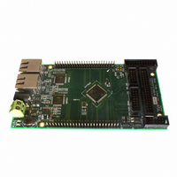
BOARD EVAL BASED ON STR912FA
Manufacturer
STMicroelectronics
Datasheets
1.STEVAL-IFW001V1.pdf
(102 pages)
2.STEVAL-IFW001V1.pdf
(9 pages)
3.STEVAL-IFW001V1.pdf
(7 pages)
Specifications of STEVAL-IFW001V1
Design Resources
STEVAL-IFW001V1 Gerber Files STEVAL-IFW001V1 Schematic STEVAL-IFW001V1 Bill of Material
Main Purpose
Interface, Ethernet
Embedded
Yes, MCU, 32-Bit
Utilized Ic / Part
E-STE101P, STR912FAW44
Primary Attributes
Dual Ethernet Transceivers for Full Duplex Communication
Secondary Attributes
Up to 32 MII Addresses, UART, I2C, SPI, with RJ45 Connectors
Silicon Manufacturer
ST Micro
Core Architecture
ARM
Core Sub-architecture
ARM9
Silicon Core Number
STR9
Silicon Family Name
STR91x
For Use With
497-8263 - BOARD EXTENSION STEVAL-IFW001V1
Lead Free Status / RoHS Status
Lead free / RoHS Compliant
Other names
497-8262


STR91xFAxxx
List of figures
Figure 1.
Figure 2.
Figure 3.
Figure 4.
Figure 5.
Figure 6.
Figure 7.
Figure 8.
Figure 9.
Figure 10.
Figure 11.
Figure 12.
Figure 13.
Figure 14.
Figure 15.
Figure 16.
Figure 17.
Figure 18.
Figure 19.
Figure 20.
Figure 21.
Figure 22.
Figure 23.
Figure 24.
Figure 25.
Figure 26.
Figure 27.
Figure 28.
Figure 29.
Figure 30.
Figure 31.
Figure 32.
Figure 33.
Figure 34.
Figure 35.
Figure 36.
Figure 37.
Figure 38.
Figure 39.
Figure 40.
Figure 41.
Figure 42.
Figure 43.
STR91xFA block diagram . . . . . . . . . . . . . . . . . . . . . . . . . . . . . . . . . . . . . . . . . . . . . . . . . . 14
Clock control . . . . . . . . . . . . . . . . . . . . . . . . . . . . . . . . . . . . . . . . . . . . . . . . . . . . . . . . . . . . 21
JTAG chaining inside the STR91xFA . . . . . . . . . . . . . . . . . . . . . . . . . . . . . . . . . . . . . . . . . 28
EMI 16-bit multiplexed connection example . . . . . . . . . . . . . . . . . . . . . . . . . . . . . . . . . . . . 40
EMI 8-bit multiplexed connection example . . . . . . . . . . . . . . . . . . . . . . . . . . . . . . . . . . . . . 40
EMI 8-bit non-multiplexed connection example . . . . . . . . . . . . . . . . . . . . . . . . . . . . . . . . . 41
STR91xFAM 80-pin package pinout . . . . . . . . . . . . . . . . . . . . . . . . . . . . . . . . . . . . . . . . . . 43
STR91xFAW 128-pin package pinout . . . . . . . . . . . . . . . . . . . . . . . . . . . . . . . . . . . . . . . . 44
STR91xFA memory map . . . . . . . . . . . . . . . . . . . . . . . . . . . . . . . . . . . . . . . . . . . . . . . . . . 57
Pin loading conditions . . . . . . . . . . . . . . . . . . . . . . . . . . . . . . . . . . . . . . . . . . . . . . . . . . . . . 58
Pin input voltage . . . . . . . . . . . . . . . . . . . . . . . . . . . . . . . . . . . . . . . . . . . . . . . . . . . . . . . . . 59
LVD reset delay case 1. . . . . . . . . . . . . . . . . . . . . . . . . . . . . . . . . . . . . . . . . . . . . . . . . . . . 63
LVD reset delay case 2. . . . . . . . . . . . . . . . . . . . . . . . . . . . . . . . . . . . . . . . . . . . . . . . . . . . 63
LVD reset delay case 3. . . . . . . . . . . . . . . . . . . . . . . . . . . . . . . . . . . . . . . . . . . . . . . . . . . . 63
Sleep mode current vs temperature with LVD on . . . . . . . . . . . . . . . . . . . . . . . . . . . . . . . . 65
Typical application with an external clock source . . . . . . . . . . . . . . . . . . . . . . . . . . . . . . . . 68
Typical application with a 32.768 kHz crystal . . . . . . . . . . . . . . . . . . . . . . . . . . . . . . . . . . . 69
Non-mux write timings . . . . . . . . . . . . . . . . . . . . . . . . . . . . . . . . . . . . . . . . . . . . . . . . . . . . 76
Non-mux bus read timings . . . . . . . . . . . . . . . . . . . . . . . . . . . . . . . . . . . . . . . . . . . . . . . . . 77
Mux write diagram . . . . . . . . . . . . . . . . . . . . . . . . . . . . . . . . . . . . . . . . . . . . . . . . . . . . . . . 78
Mux read diagram . . . . . . . . . . . . . . . . . . . . . . . . . . . . . . . . . . . . . . . . . . . . . . . . . . . . . . . . 79
Page mode read diagram . . . . . . . . . . . . . . . . . . . . . . . . . . . . . . . . . . . . . . . . . . . . . . . . . . 80
Sync burst write diagram . . . . . . . . . . . . . . . . . . . . . . . . . . . . . . . . . . . . . . . . . . . . . . . . . . 81
Sync burst read diagram. . . . . . . . . . . . . . . . . . . . . . . . . . . . . . . . . . . . . . . . . . . . . . . . . . . 83
MII_RX_CLK and MII_TX_CLK timing diagram . . . . . . . . . . . . . . . . . . . . . . . . . . . . . . . . . 84
MDC timing diagram . . . . . . . . . . . . . . . . . . . . . . . . . . . . . . . . . . . . . . . . . . . . . . . . . . . . . . 84
Ethernet MII management timing diagram . . . . . . . . . . . . . . . . . . . . . . . . . . . . . . . . . . . . . 85
Ethernet MII transmit timing diagram . . . . . . . . . . . . . . . . . . . . . . . . . . . . . . . . . . . . . . . . . 85
Ethernet MII receive timing diagram . . . . . . . . . . . . . . . . . . . . . . . . . . . . . . . . . . . . . . . . . . 86
SPI slave timing diagram with CPHA = 0 . . . . . . . . . . . . . . . . . . . . . . . . . . . . . . . . . . . . . . 88
SPI slave timing diagram with CPHA = 1 . . . . . . . . . . . . . . . . . . . . . . . . . . . . . . . . . . . . . . 89
SPI master timing diagram . . . . . . . . . . . . . . . . . . . . . . . . . . . . . . . . . . . . . . . . . . . . . . . . 89
ADC conversion characteristics . . . . . . . . . . . . . . . . . . . . . . . . . . . . . . . . . . . . . . . . . . . . . 92
Device marking for revision G LQFP80 and LQFP128 packages. . . . . . . . . . . . . . . . . . . . 93
Device marking for revision G LFBGA144 packages . . . . . . . . . . . . . . . . . . . . . . . . . . . . . 93
Device marking for revision H LQFP80 and LQFP128 packages. . . . . . . . . . . . . . . . . . . . 93
Device marking for revision H LFBGA144 packages . . . . . . . . . . . . . . . . . . . . . . . . . . . . . 93
Device marking for revision A LQFP80 and LQFP128 packages . . . . . . . . . . . . . . . . . . . . 94
Device marking for revision A LFBGA144 packages . . . . . . . . . . . . . . . . . . . . . . . . . . . . . 94
80-pin low profile quad flat package (LQFP80) outline . . . . . . . . . . . . . . . . . . . . . . . . . . . . 95
128-pin low profile quad flat package (LQFP128) outline . . . . . . . . . . . . . . . . . . . . . . . . . . 96
144-ball low profile fine pitch ball grid array package (LFBGA144) outline . . . . . . . . . . . . 97
Recommended PCB design rules (0.80/0.75 mm pitch BGA) . . . . . . . . . . . . . . . . . . . . . . 98
Doc ID 13495 Rev 6
List of figures
9/102
Related parts for STEVAL-IFW001V1
Image
Part Number
Description
Manufacturer
Datasheet
Request
R

Part Number:
Description:
BOARD EVAL SPZB260 MOD FOR STR9
Manufacturer:
STMicroelectronics
Datasheet:

Part Number:
Description:
BOARD EVAL EXTENSION SN250
Manufacturer:
STMicroelectronics
Datasheet:

Part Number:
Description:
BOARD EVAL AB-54003L-512
Manufacturer:
STMicroelectronics
Datasheet:

Part Number:
Description:
BOARD REF DESIGN RF DMOS PWR AMP
Manufacturer:
STMicroelectronics
Datasheet:

Part Number:
Description:
BOARD EVAL PWR AMP AB-84008L-470
Manufacturer:
STMicroelectronics
Datasheet:

Part Number:
Description:
BOARD EVAL FOR STM32F103XX
Manufacturer:
STMicroelectronics
Datasheet:

Part Number:
Description:
BOARD EVAL AB-54003L-512
Manufacturer:
STMicroelectronics
Datasheet:

Part Number:
Description:
BOARD SMART PLUG STM32 SPZB260PR
Manufacturer:
STMicroelectronics
Datasheet:

Part Number:
Description:
BOARD DEMO BLUETOOTH SPBT2532C2
Manufacturer:
STMicroelectronics
Datasheet:
Part Number:
Description:
ZIGBEE USB DONGLE EVAL KIT
Manufacturer:
STMicroelectronics
Datasheet:
Part Number:
Description:
STMicroelectronics [RIPPLE-CARRY BINARY COUNTER/DIVIDERS]
Manufacturer:
STMicroelectronics
Datasheet:
Part Number:
Description:
STMicroelectronics [LIQUID-CRYSTAL DISPLAY DRIVERS]
Manufacturer:
STMicroelectronics
Datasheet:

Part Number:
Description:
BOARD EVAL FOR MEMS SENSORS
Manufacturer:
STMicroelectronics
Datasheet: