STEVAL-IFW001V1 STMicroelectronics, STEVAL-IFW001V1 Datasheet - Page 56
STEVAL-IFW001V1
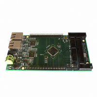
Manufacturer Part Number
STEVAL-IFW001V1
Description
BOARD EVAL BASED ON STR912FA
Manufacturer
STMicroelectronics
Datasheets
1.STEVAL-IFW001V1.pdf
(102 pages)
2.STEVAL-IFW001V1.pdf
(9 pages)
3.STEVAL-IFW001V1.pdf
(7 pages)
Specifications of STEVAL-IFW001V1
Design Resources
STEVAL-IFW001V1 Gerber Files STEVAL-IFW001V1 Schematic STEVAL-IFW001V1 Bill of Material
Main Purpose
Interface, Ethernet
Embedded
Yes, MCU, 32-Bit
Utilized Ic / Part
E-STE101P, STR912FAW44
Primary Attributes
Dual Ethernet Transceivers for Full Duplex Communication
Secondary Attributes
Up to 32 MII Addresses, UART, I2C, SPI, with RJ45 Connectors
Silicon Manufacturer
ST Micro
Core Architecture
ARM
Core Sub-architecture
ARM9
Silicon Core Number
STR9
Silicon Family Name
STR91x
For Use With
497-8263 - BOARD EXTENSION STEVAL-IFW001V1
Lead Free Status / RoHS Status
Lead free / RoHS Compliant
Other names
497-8262


Memory mapping
6.5
56/102
If the main Flash contents are incorrect, the CPU, while executing code from the secondary
Flash, can download new data from any STR91xFA communication channel and program
into primary Flash memory. Application code then starts after the new contents of primary
Flash are verified.
STR91xFA memory map
The memory map is shown in
●
●
●
●
Either of the two Flash memories may be placed at CPU boot address 0x0000.0000.
By default, the primary Flash memory is in boot position starting at CPU address
0x0000.0000 and the secondary Flash memory may be placed at a higher address
following the end of the primary Flash memory. This default option may be changed
using the STR91xx device configuration software, placing the secondary Flash memory
at CPU boot location 0x0000.0000, and then the primary Flash memory may be placed
at a higher address.
The local SRAM (64KB or 96KB) is aliased in three address windows. A) At
0x0400.0000 the SRAM is accessible through the CPU’s D-TCM, at 0x4000.0000 the
SRAM is accessible through the CPU’s AHB in buffered accesses, and at 0x5000.0000
the SRAM is accessible through the CPU’s AHB in non-buffered accesses. An AHB bus
master other than the CPU can access SRAM in all three aliased windows, but these
accesses are always non-buffered. The CPU is the only AHB master that can
performed buffered writes.
APB peripherals reside in two AHB-to-APB peripheral bridge address windows, APB0
and APB1. These peripherals are accessible with buffered AHB access if the CPU
addresses them in the address range of 0x4800.0000 to 0x4FFF.FFFF, and non-
buffered access in the address range of 0x5800.0000 to 0x5FFF.FFFF.
Individual peripherals on the APB are accessed at the listed address offset plus the
base address of the appropriate AHB-to-APB bridge.
Figure 9: STR91xFA memory map on page
Doc ID 13495 Rev 6
57:
STR91xFAxxx
Related parts for STEVAL-IFW001V1
Image
Part Number
Description
Manufacturer
Datasheet
Request
R

Part Number:
Description:
BOARD EVAL SPZB260 MOD FOR STR9
Manufacturer:
STMicroelectronics
Datasheet:

Part Number:
Description:
BOARD EVAL EXTENSION SN250
Manufacturer:
STMicroelectronics
Datasheet:

Part Number:
Description:
BOARD EVAL AB-54003L-512
Manufacturer:
STMicroelectronics
Datasheet:

Part Number:
Description:
BOARD REF DESIGN RF DMOS PWR AMP
Manufacturer:
STMicroelectronics
Datasheet:

Part Number:
Description:
BOARD EVAL PWR AMP AB-84008L-470
Manufacturer:
STMicroelectronics
Datasheet:

Part Number:
Description:
BOARD EVAL FOR STM32F103XX
Manufacturer:
STMicroelectronics
Datasheet:

Part Number:
Description:
BOARD EVAL AB-54003L-512
Manufacturer:
STMicroelectronics
Datasheet:

Part Number:
Description:
BOARD SMART PLUG STM32 SPZB260PR
Manufacturer:
STMicroelectronics
Datasheet:

Part Number:
Description:
BOARD DEMO BLUETOOTH SPBT2532C2
Manufacturer:
STMicroelectronics
Datasheet:
Part Number:
Description:
ZIGBEE USB DONGLE EVAL KIT
Manufacturer:
STMicroelectronics
Datasheet:
Part Number:
Description:
STMicroelectronics [RIPPLE-CARRY BINARY COUNTER/DIVIDERS]
Manufacturer:
STMicroelectronics
Datasheet:
Part Number:
Description:
STMicroelectronics [LIQUID-CRYSTAL DISPLAY DRIVERS]
Manufacturer:
STMicroelectronics
Datasheet:

Part Number:
Description:
BOARD EVAL FOR MEMS SENSORS
Manufacturer:
STMicroelectronics
Datasheet: