STEVAL-IFW001V1 STMicroelectronics, STEVAL-IFW001V1 Datasheet - Page 27
STEVAL-IFW001V1
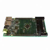
Manufacturer Part Number
STEVAL-IFW001V1
Description
BOARD EVAL BASED ON STR912FA
Manufacturer
STMicroelectronics
Datasheets
1.STEVAL-IFW001V1.pdf
(102 pages)
2.STEVAL-IFW001V1.pdf
(9 pages)
3.STEVAL-IFW001V1.pdf
(7 pages)
Specifications of STEVAL-IFW001V1
Design Resources
STEVAL-IFW001V1 Gerber Files STEVAL-IFW001V1 Schematic STEVAL-IFW001V1 Bill of Material
Main Purpose
Interface, Ethernet
Embedded
Yes, MCU, 32-Bit
Utilized Ic / Part
E-STE101P, STR912FAW44
Primary Attributes
Dual Ethernet Transceivers for Full Duplex Communication
Secondary Attributes
Up to 32 MII Addresses, UART, I2C, SPI, with RJ45 Connectors
Silicon Manufacturer
ST Micro
Core Architecture
ARM
Core Sub-architecture
ARM9
Silicon Core Number
STR9
Silicon Family Name
STR91x
For Use With
497-8263 - BOARD EXTENSION STEVAL-IFW001V1
Lead Free Status / RoHS Status
Lead free / RoHS Compliant
Other names
497-8262


STR91xFAxxx
3.13.7
3.14
3.15
Tamper detection
On 128-pin and 144-ball STR91xFA devices only, there is a tamper detect input pin,
TAMPER_IN, used to detect and record the time of a tamper event on the end product such
as malicious opening of an enclosure, unwanted opening of a panel, etc. The activation
mode of the tamper pin detects when a signal on the tamper input pin is driven from low-to-
high, or high-to-low depending on firmware configuration. Once a tamper event occurs, the
RTC time (millisecond resolution) and the date are recorded in the RTC unit.
Simultaneously, the SRAM standby voltage source will be cut off to invalidate all SRAM
contents. Tamper detection control and status logic are part of the RTC unit.
Real-time clock (RTC)
The RTC combines the functions of a complete time-of-day clock (millisecond resolution)
with an alarm programmable up to one month, a 9999-year calender with leap-year support,
periodic interrupt generation from 1 to 512 Hz, tamper detection (described in
Section
hour mode, and time/calendar values are stored in binary-coded decimal format.
The RTC also provides a self-isolation mode that is automatically activated during power
down. This feature allows the RTC to continue operation when V
as long as an alternate power source, such as a battery, is connected to the VBATT input
pin. The current drawn by the RTC unit on the VBATT pin is very low in this standby mode,
I
JTAG interface
An IEEE-1149.1 JTAG interface on the STR91xFA provides In-System-Programming (ISP)
of all memory, boundary scan testing of pins, and the capability to debug the CPU.
STR91xFA devices are shipped from ST with blank Flash memories. The CPU can only boot
from Flash memory (selection of which Flash bank is programmable). Firmware must be
initially programmed through JTAG into one of these Flash memories before the STR91xFA
is used.
Six pins are used on this JTAG serial interface. The five signals JTDI, JTDO, JTMS, JTCK,
and JTRSTn are all standard JTAG signals complying with the IEEE-1149.1 specification.
The sixth signal, JRTCK (Return TCK), is an output from the STR91xFA and it is used to
pace the JTCK clock signal coming in from the external JTAG test equipment for debugging.
The frequency of the JTCK clock signal coming from the JTAG test equipment must be at
least 10 times less than the ARM966E-S CPU core operating frequency (f
ensure this, the signal JRTCK is output from the STR91xFA and is input to the external
JTAG test equipment to hold off transitions of JTCK until the CPU core is ready, meaning
that the JTAG equipment cannot send the next rising edge of JTCK until the equipment
receives a rising edge of JRTCK from the STR91xFA. The JTAG test equipment must be
able to interpret the signal JRTCK and perform this adaptive clocking function. If it is known
that the CPU clock will always be at least ten times faster than the incoming JTCK clock
signal, then the JRTCK signal is not needed.
The two die inside the STR91xFA (CPU die and Flash memory die) are internally daisy-
chained on the JTAG bus, see
Ports (TAPs), one for boundary scan functions and one for ARM CPU debug. The Flash
memory die has one TAP for program/erase of non-volatile memory. Because these three
RTC_STBY
3.13.7), and an optional clock calibration output on the JRTCK pin. The time is in 24
.
Figure 3 on page
Doc ID 13495 Rev 6
28. The CPU die has two JTAG Test Access
DDQ
and V
Functional overview
CPUCLK
DD
are absent,
). To
27/102
Related parts for STEVAL-IFW001V1
Image
Part Number
Description
Manufacturer
Datasheet
Request
R

Part Number:
Description:
BOARD EVAL SPZB260 MOD FOR STR9
Manufacturer:
STMicroelectronics
Datasheet:

Part Number:
Description:
BOARD EVAL EXTENSION SN250
Manufacturer:
STMicroelectronics
Datasheet:

Part Number:
Description:
BOARD EVAL AB-54003L-512
Manufacturer:
STMicroelectronics
Datasheet:

Part Number:
Description:
BOARD REF DESIGN RF DMOS PWR AMP
Manufacturer:
STMicroelectronics
Datasheet:

Part Number:
Description:
BOARD EVAL PWR AMP AB-84008L-470
Manufacturer:
STMicroelectronics
Datasheet:

Part Number:
Description:
BOARD EVAL FOR STM32F103XX
Manufacturer:
STMicroelectronics
Datasheet:

Part Number:
Description:
BOARD EVAL AB-54003L-512
Manufacturer:
STMicroelectronics
Datasheet:

Part Number:
Description:
BOARD SMART PLUG STM32 SPZB260PR
Manufacturer:
STMicroelectronics
Datasheet:

Part Number:
Description:
BOARD DEMO BLUETOOTH SPBT2532C2
Manufacturer:
STMicroelectronics
Datasheet:
Part Number:
Description:
ZIGBEE USB DONGLE EVAL KIT
Manufacturer:
STMicroelectronics
Datasheet:
Part Number:
Description:
STMicroelectronics [RIPPLE-CARRY BINARY COUNTER/DIVIDERS]
Manufacturer:
STMicroelectronics
Datasheet:
Part Number:
Description:
STMicroelectronics [LIQUID-CRYSTAL DISPLAY DRIVERS]
Manufacturer:
STMicroelectronics
Datasheet:

Part Number:
Description:
BOARD EVAL FOR MEMS SENSORS
Manufacturer:
STMicroelectronics
Datasheet: