STEVAL-IFW001V1 STMicroelectronics, STEVAL-IFW001V1 Datasheet - Page 35
STEVAL-IFW001V1
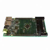
Manufacturer Part Number
STEVAL-IFW001V1
Description
BOARD EVAL BASED ON STR912FA
Manufacturer
STMicroelectronics
Datasheets
1.STEVAL-IFW001V1.pdf
(102 pages)
2.STEVAL-IFW001V1.pdf
(9 pages)
3.STEVAL-IFW001V1.pdf
(7 pages)
Specifications of STEVAL-IFW001V1
Design Resources
STEVAL-IFW001V1 Gerber Files STEVAL-IFW001V1 Schematic STEVAL-IFW001V1 Bill of Material
Main Purpose
Interface, Ethernet
Embedded
Yes, MCU, 32-Bit
Utilized Ic / Part
E-STE101P, STR912FAW44
Primary Attributes
Dual Ethernet Transceivers for Full Duplex Communication
Secondary Attributes
Up to 32 MII Addresses, UART, I2C, SPI, with RJ45 Connectors
Silicon Manufacturer
ST Micro
Core Architecture
ARM
Core Sub-architecture
ARM9
Silicon Core Number
STR9
Silicon Family Name
STR91x
For Use With
497-8263 - BOARD EXTENSION STEVAL-IFW001V1
Lead Free Status / RoHS Status
Lead free / RoHS Compliant
Other names
497-8262


STR91xFAxxx
3.22.1
3.23
3.24
DMA
A programmable DMA channel may be assigned by CPU firmware to service each SSP
channel for fast and direct transfers between the SSP bus and SRAM with little CPU
involvement. Both DMA single-transfers and DMA burst-transfers are supported for transmit
and receive. Burst transfers require that FIFOs are enabled.
General purpose I/O
There are up to 80 GPIO pins available on 10 I/O ports for 128-pin and 144-ball devices, and
up to 40 GPIO pins on 5 I/O ports for 80-pin devices. Each and every GPIO pin by default
(during and just after a reset condition) is in high-impedance input mode, and some GPIO
pins are additionally routed to certain peripheral function inputs. CPU firmware may initialize
GPIO pins to have alternate input or output functions as listed in
logic state of any GPIO pin may be read by firmware as a GPIO input, regardless of its
reassigned input or output function.
Bit masking is available on each port, meaning firmware may selectively read or write
individual port pins, without disturbing other pins on the same port during a write.
Firmware may designate each GPIO pin to have open-drain or push-pull characteristics.
All GPIO pins are 5 V tolerant, meaning they can drive a voltage level up to VDDQ, and can
be safely driven by a voltage up to 5 V.
A/D converter (ADC) with DMA
The STR91xFA provides an eight-channel, 10-bit successive approximation analog-to-
digital converter. The ADC input pins are multiplexed with other functions on Port 4 as
shown in
●
●
●
●
●
●
●
●
Fast conversion time, as low as 0.7 usec
Accuracy. Integral and differential non-linearity are typically within 4 conversion counts.
0 to 3.6 V input range. External reference voltage input pin (AVREF) available on 128-
pin packages for better accuracy on low-voltage inputs. See
conditions, for restrictions to the relative voltage levels of VDDQ, AVDD, AVREF, and
AVREF_AVDD.
CPU Firmware may convert one ADC input channel at a time, or it has the option to set
the ADC to automatically scan and convert all eight ADC input channels sequentially
before signalling an end-of-conversion
Automatic continuous conversion mode is available for any number of designated ADC
input channels
Analog watchdog mode provides automatic monitoring of any ADC input, comparing it
against two programmable voltage threshold values. The ADC unit will set a flag or it
will interrupt the CPU if the input voltage rises above the higher threshold, or drops
below the lower threshold.
The ADC unit goes to stand-by mode (very low-current consumption) after any reset
event. CPU firmware may also command the ADC unit to stand-by mode at any time.
ADC conversion can be started or triggered by software command as well as triggers
from Timer/Counter (TIM), Motor Controller and input from external pin.
Table
8. Following are the major ADC features:
Doc ID 13495 Rev 6
Table
Table 11: Operating
Functional overview
8. At any time, the
35/102
Related parts for STEVAL-IFW001V1
Image
Part Number
Description
Manufacturer
Datasheet
Request
R

Part Number:
Description:
BOARD EVAL SPZB260 MOD FOR STR9
Manufacturer:
STMicroelectronics
Datasheet:

Part Number:
Description:
BOARD EVAL EXTENSION SN250
Manufacturer:
STMicroelectronics
Datasheet:

Part Number:
Description:
BOARD EVAL AB-54003L-512
Manufacturer:
STMicroelectronics
Datasheet:

Part Number:
Description:
BOARD REF DESIGN RF DMOS PWR AMP
Manufacturer:
STMicroelectronics
Datasheet:

Part Number:
Description:
BOARD EVAL PWR AMP AB-84008L-470
Manufacturer:
STMicroelectronics
Datasheet:

Part Number:
Description:
BOARD EVAL FOR STM32F103XX
Manufacturer:
STMicroelectronics
Datasheet:

Part Number:
Description:
BOARD EVAL AB-54003L-512
Manufacturer:
STMicroelectronics
Datasheet:

Part Number:
Description:
BOARD SMART PLUG STM32 SPZB260PR
Manufacturer:
STMicroelectronics
Datasheet:

Part Number:
Description:
BOARD DEMO BLUETOOTH SPBT2532C2
Manufacturer:
STMicroelectronics
Datasheet:
Part Number:
Description:
ZIGBEE USB DONGLE EVAL KIT
Manufacturer:
STMicroelectronics
Datasheet:
Part Number:
Description:
STMicroelectronics [RIPPLE-CARRY BINARY COUNTER/DIVIDERS]
Manufacturer:
STMicroelectronics
Datasheet:
Part Number:
Description:
STMicroelectronics [LIQUID-CRYSTAL DISPLAY DRIVERS]
Manufacturer:
STMicroelectronics
Datasheet:

Part Number:
Description:
BOARD EVAL FOR MEMS SENSORS
Manufacturer:
STMicroelectronics
Datasheet: