DLP-2232M-G DLP Design Inc, DLP-2232M-G Datasheet
DLP-2232M-G
Specifications of DLP-2232M-G


Related parts for DLP-2232M-G


DLP-2232M-G Summary of contents
Page 1
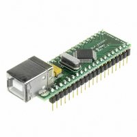
... Multi-Protocol Synchronous Serial Engine interface designed specifically for synchronous serial protocols such as JTAG and SPI bus. The DLP-2232M-G features a quality four-layer printed circuit board with a solid ground plane, an integral 93C56 EEPROM on board for easy OEM customization and a standard 40-pin, 0.6in wide footprint. Integral power control and on-board MOSFET power switch make the DLP-2232M-G a perfect choice for USB bus-powered, high-power designs as well as self- and low-powered products ...
Page 2
... USB Dual Port RS422 / RS485 • Upgrading Legacy Peripheral Designs • USB Instrumentation • USB JTAG Programming • USB to SPI Bus Interfaces • USB Industrial Control • Field Upgradeable USB Products • Galvanically Isolated Products With USB Interface 2 DLP-2232M-G DLP Design, Inc. ...
Page 3
... General Description The DLP-2232M-G module is a USB interface that incorporates the functionality of two DLP-USB2xxM modules into a single 40-pin module. A single downstream USB port is converted to two IO channels that can each be individually configured as a DLP- USB232M-style UART interface DLP-USB245M-style FIFO interface, without the need to add a USB hub ...
Page 4
... MCU and other devices. • Integrated level converter on UART / FIFO interface and control signals Each channel of the DLP-2232M-G has its own independent VCCIO pin that can be supplied by between 3V to 5V. This allows each channel’s output voltage drive level to be individually configured. Thus allowing, for example, 3.3V logic to be interfaced to the device without the need for external level converter I.C.’ ...
Page 5
... Enhanced Asynchronous Bit-Bang Interface The DLP-2232M-G supports FTDI’s BM chip Bit Bang mode. In Bit Bang mode, the eight FIFO data lines can be switched between FIFO interface mode and an 8-bit Parallel IO port. Data packets can be sent to the device and they will be sequentially sent to the interface at a rate controlled by an internal timer (equivalent to the baud rate prescaler) ...
Page 6
... This new mode combines the ‘A’ and ‘B’ bus interface to make the DLP-2232M-G interface emulate a standard 8048 / 8051 style MCU bus. This allows peripheral devices for these MCU families to be directly attached to the DLP-2232M-G with IO being performed over USB with the help of MPSSE interface technology. ...
Page 7
... DLP-2232M-G Module Simplified Block Diagram USB Type 'B' connector to Host PC/Mac 6MHz Resonator 3.1 Functional Block Descriptions • 6MHz Oscillator The 6MHz Oscillator cell generates a 6MHz reference clock input to the x8 Clock multiplier from an external 6MHz ceramic resonator. • Multi-Purpose UART / FIFO Controllers The Multi-purpose UART / FIFO controllers handle the transfer of data between the Dual Port RX and TX buffers and the UART / FIFO transmit and receive registers ...
Page 8
... The UARTs also support the RS232 BREAK setting and detection conditions. • EEPROM Interface The on-board 93C56 EEPROM allows each of the DLP-2232M-G module’s channels to be independently configured as a serial UART (232 mode parallel FIFO (245 mode). The EEPROM is used to enable the CPU-style FIFO interface, and Fast Opto- Isolated Serial interface modes ...
Page 9
... I/O pins are defined by chip mode. More detailed descriptions of the operation of the I/O pins are provided in section x. (was 9) 4.2 Common Pins The operation of the following DLP-2232M-G pins stay the same, regardless of the operating mode. Pin# Signal ...
Page 10
... D7 GPIOL3 CS# WR# *Note 6 GPIOH0 A0 RD# *Note 6 GPIOH1 RD# WR# *Note 7 GPIOH2 WR# RD# *Note 7 GPIOH3 SI/WUA SI/WUA 10 DLP-2232M-G DLP Design, Inc. Fast MCU Host Opto- Bus Isolated Enumeration Serial Mode Mode *Note 5 AD0 *Note 3 AD1 AD2 AD3 AD4 AD5 AD6 AD7 I/O0 I/O1 ...
Page 11
... Bit-Bang Modes CS# WR# *Note 8 A0 RD# *Note 8 RD# WR# *Note 7 WR# RD# *Note 7 SI/WUB 11 DLP-2232M-G DLP Design, Inc. Fast MCU Host Opto- Bus Isolated Enumeration Serial Mode Mode *Note 5 AD8 FSDI AD9 FSCLK AD10 FSDO AD11 FSCTS AD12 *Note 3 AD13 AD14 AD15 CS# ALE RD# WR# ...
Page 12
... PCB Rev 1.6 (May 2009) 0.1 typ. (2.54 typ.) 0.25 typ. (6.4typ.) 0.50 typ. (12.7 typ.) ** 0.6 typ. (15.2 typ.) 0.7 typ. (17.8 typ.) 12 DLP-2232M-G DLP Design, Inc. 0.65 typ. (16.5 typ.) 0.36 typ. (9.1 typ.) ...
Page 13
... V I source = 2mA 0.3 0.4 0 sink = 2mA 1.3 1.6 1.9 V *Note *Note 12 Min Typ Max Units Conditions 2.2 2.7 3 source = 1mA 0.3 0.4 0 sink = 2mA *Note 13 1.0 1.2 1 Min Typ Max Units Conditions 1.3 1.6 1 DLP-2232M-G DLP Design, Inc *Note 11 ...
Page 14
... Figure 8a - USB Bus Powered Configuration Figure 8a illustrates the DLP-2232M typical USB bus powered configuration. A USB Bus Powered device gets its power from the USB bus. Basic rules for USB Bus power devices are as follows – plug-in, the device must draw no more than 100mA b) On USB Suspend the device must draw no more than 500uA ...
Page 15
... USBDP via the 1.5K pull-up resistor when the host or hub is powered down. Failure to do this may cause some USB host or hub controllers to power up erratically. When the DLP-2232M reset, the I/O interface pins all go tri-state. These Note: pins have 200K pull-up resistors to VCCIOx internal to the FT2232D, so they will gently pull high unless driven by some external logic ...
Page 16
... USB Bus-Powered, 5V Systems Rev 1.6 (May 2009) 5V Microcontroller Systems 1 6.000 External 5V Supply Figure 10b - Self Powered 3.3 Volt Microcontroller Systems 1 External 5V Supply 6.000 External 3.3V Supply Figure 10d - Self Powered 16 DLP-2232M-G DLP Design, Inc. 40 External 5V Supply Microcontroller VCC 21 External 40 3.3V Supply Microcontroller VCC 21 ...
Page 17
... VCCIOx pin. 8.2.4 USB Self-Powered, 3.3V Systems Figure 10d is an example of a DLP-2232M-G USB self-powered design with 3.3V interface. In this case, the VCCIOA and VCCIOB pins are supplied by an external 3.3V supply in order to make both of the device’s IO channels drive out at 3.3V logic level, Rev 1 ...
Page 18
... Data Set Ready Control Input / Handshake signal 9 INPUT Data Carrier Detect Control Input INPUT Ring Indicator Control Input. When the Remote Wake up option is enabled in the EEPROM, taking RI# low can be used to resume the PC USB Host controller from suspend. *Note 9 18 DLP-2232M-G DLP Design, Inc. *Note 9 *Note *Note *Note 9 ...
Page 19
... TX buffer will be sent out over USB on the next Bulk-IN request from the drivers regardless of the pending packet size. This can be used to optimize USB transfer speed for some applications. Tie this pin to VCCIOx if not used. 19 DLP-2232M-G DLP Design, Inc. * Note 11 * Note 11 * Note 10 ...
Page 20
... Load 30 pF 9.3.2 FIFO Write Cycle Timing TXE# WR D[7...0] Time Description WR# Active Pulse Width Pre-Charge Time Data Setup Time before WR inactive T9 Rev 1.6 (May 2009) T1 Valid Data ** Note 12 ** Note 12 T11 T7 T9 Valid Data 20 DLP-2232M-G DLP Design, Inc Min Max Unit T12 ...
Page 21
... Enhanced Asynchronous and Synchronous Bit-Bang Modes - Signal Description and Interface Configuration Bit-bang mode is a special DLP-2232M-G mode that changes the 8 IO lines on either or both channels (A/B) into an 8 bit bi-directional bus. There are now two types of bit bang modes - Enhanced Asynchronous, which is virtually the same as BM-style Bit-Bang mode ...
Page 22
... Enhanced Asynchronous Bit-Bang Mode Enhanced Asynchronous Bit-Bang mode is the same as BM-style Bit-Bang mode, except that the internal RD# and WR# strobes are now brought out of the DLP-2232M-G to allow external logic to be clocked by accesses to the bit-bang IO bus. On either or both channels, any data written to the device in the normal manner will be self clocked onto the data pins (those which have been configured as outputs) ...
Page 23
... The internal RD# and WR# strobes are brought off-board to allow external logic to be clocked by accesses to the bit-bang IO bus. Enabling Synchronous Bit-Bang mode is enabled by the Set Bit Bang Mode command: Set_USB_Device_BitMode($00,$04 enable it Set_USB_Device_BitMode($00,$00 reset it Rev 1.6 (May 2009 New Data 23 DLP-2232M-G DLP Design, Inc. ...
Page 24
... JTAG and SPI Bus. It can also be used to program SRAM based FPGA’s over USB. The MPSSE interface is designed to be flexible so that it can be configured to allow any synchronous serial protocol (industry standard or proprietary interfaced to the DLP-2232M-G. MPSSE is available on channel A only. MPSSE is fully configurable, and is programmed by sending commands down the data pipe ...
Page 25
... Read Extended (changes A15 to A8) 3) Write (does not change A15 to A8) 4) Write Extended (changes A15 to A8) Enabling MCU Host Bus Emulation Mode enabled using the Set Bit-Bang Mode command. Set_USB_Device_BitMode($00,$08 enable it Set_USB_Device_BitMode($00,$00 reset it Rev 1.6 (May 2009) 25 DLP-2232M-G DLP Design, Inc. ...
Page 26
... PC. I/O1 must be held in input mode if this option is used. *Note Extends the time taken to perform a Read or Write operation if pulled low. Pull up to Vcc if not being used. low, and is held after WR# goes high) No Connect 26 DLP-2232M-G DLP Design, Inc. ...
Page 27
... WR# is driven active low. This will extend to 6 clocks wide if IORDY# is low. t9 WR# is driven inactive high. t10 CS# is driven inactive, 1/2 a clock period after WR# goes inactive t11 Data is held until here and may now change Rev 1.6 (May 2009 High Address Low Address Data 27 DLP-2232M-G DLP Design, Inc t10 t11 ...
Page 28
... Figure 31 - MCU Host Bus Emulation Mode Signal Timing - Clock (OSC) Signal t high OSC Time Description tperiod Clock Period Rev 1.6 (May 2009 High Address Hi-Z Low Address t t period low Typical Value ?? 28 DLP-2232M-G DLP Design, Inc Unit ns ...
Page 29
... This gives the external device full control over the interface designed to be half duplex so that data is only transferred in one direction at a time. chip is ready to send data. 29 DLP-2232M-G DLP Design, Inc ...
Page 30
... The source bit (SRCE) indicates which channel the data has come from. A ‘0’ means that it has come from Channel A, a ‘1’ means that it has come from Channel B. Rev 1.6 (May 2009 Min Data Bits - LSB first 30 DLP-2232M-G DLP Design, Inc. Max Unit SRCE Source Bit ...
Page 31
... B. A ‘1’ will send it to channel B, providing channel B is enabled for fast serial mode, otherwise it will go to channel A. Either channel A, or channel B, or both must be enabled as fast serial mode or the circuit is disabled. Figure 35 - Fast Opto-Isolated Serial Data Format - Data input to the DLP-2232M-G FSCTS FSCLK ...
Page 32
... This document provides information that may be subject to change without notice. 11.0 Contact Information DLP Design, Inc. 1605 Roma Lane Allen, TX 75013 Phone: 469-964-8027 Fax: 415-901-4859 E-Mail ( Sales ) : sales@dlpdesign.com E-Mail ( Support ) : support@dlpdesign.com Web Site URL : http://www.dlpdesign.com Rev 1.6 (May 2009) 32 DLP-2232M-G DLP Design, Inc. ...
Page 33
AGND 9 GND 18 GND 25 GND 34 GND AVCC 3 VCC 42 VCC 14 VCCIOA 31 VCCIOB 2 ...