DLP-FPGA DLP Design Inc, DLP-FPGA Datasheet
DLP-FPGA
Specifications of DLP-FPGA


Related parts for DLP-FPGA


DLP-FPGA Summary of contents
Page 1
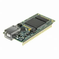
... On-Board 128K x 8, 70nS SRAM - USB Port Powered - USB 1.1 and 2.0 Compatible Interface - Small Footprint: 2.8 x 1.-Inch PCB - Standard 50-Pin, 0.9-Inch DIP Interface LEAD-FREE VREGs 50-pin, 0.9-inch Wide Interface XILINX Headers FPGA XC3S250E -4TQ144 128K x 8 SRAM © DLP Design, Inc ...
Page 2
... JTAG and SPI Flash interface ports for connection to Xilinx programming tools. 2.0 TRAINING MANUAL A 200+ page training manual for the DLP-FPGA is also available. While this manual is designed to provide entry-level instruction for those new to designing with FPGAs recommended for developers who have some experience with FPGA products and associated development tools. An ISE™ ...
Page 3
... DCM’s: 4 4.0 BITLOADAPP SOFTWARE Windows software is provided for use with the DLP-FPGA that will load an FPGA configuration (.bit) file directly to the SPI Flash device via the USB interface. This app (shown below) will allow the user to erase the flash, verify the erasure and then program and verify the flash: Rev ...
Page 4
... SPI flash. Once written to the SPI flash, the configuration will load to the FPGA and execute. Alternatively, a traditional JTAG header location is provided on the DLP-FPGA giving the user access to the pins on the FPGA required by the development tools. (Refer to the schematic at the end of this datasheet for details ...
Page 5
... LPT). 9.0 USING THE DLP-FPGA Select a power source via Header Pins 23 and 24, and connect the DLP-FPGA to the PC to initiate the loading of USB drivers. The easiest way to do this is to connect Pins 23 and 24 to each other. This will result in operational power being taken from the host PC. Once the drivers are loaded, the DLP-FPGA is ready for use ...
Page 6
... U5 Pin 31 JP2 Pin 46 U5 Pin 36 JP2 Pin 45 U5 Pin 38 JP2 Pin 44 U5 Pin 41 JP2 Pin 43 U5 Pin 47 JP2 Pin 42 U5 Pin 48 JP2 Pin 41 U5 Pin 66 JP2 Pin 39 U5 Pin 69 JP2 Pin 38 n/a n/a n/a n/a 1,11,25,26,40,50 128 © DLP Design, Inc. ...
Page 7
... Rev. 1.4 (November 2010) 0.1 typ (2.5 typ) 1.2 typ (30.5 typ) 7 0.65 typ (16.5 typ) 0.44 typ (11.2 typ) 0.29 typ (7.3 typ) .9 typ (22.9 typ) 1.2 typ (30.5 typ) © DLP Design, Inc. ...
Page 8
... This product and its documentation are supplied on an as-is basis, and no warranty as to their suitability for any particular purpose is either made or implied. DLP Design, Inc. will not accept any claim for damages whatsoever arising as a result of the use or failure of this product. Your statutory rights are not affected ...
Page 9
AGND 9 GND 18 GND 25 GND 34 GND AVCC 3 VCC 42 VCC 14 VCCIOA 31 VCCIOB ...
Page 10
VSS VCC ...