DLP-HS-FPGA DLP Design Inc, DLP-HS-FPGA Datasheet
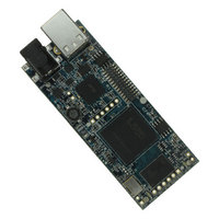
DLP-HS-FPGA
Specifications of DLP-HS-FPGA
Available stocks


Related parts for DLP-HS-FPGA


DLP-HS-FPGA Summary of contents
Page 1
... High Speed USB 2.0 Interface - 66 MHz oscillator - 133 MHz DDR2 interface reference design provided - USB Port Powered or 5V External Power Barrel Jack - USB 1.1 and 2.0 Compatible Interface - Small Footprint: 3.0 x 1.2 Inch PCB - Standard 50-Pin, 0.9-Inch DIP Interface LEAD-FREE © DLP Design, Inc ...
Page 2
... SPI Flash—no external programmer is required. This represents a savings of as much as $200 in that no additional programming cable is required for configuring the FPGA. All that is needed to load bit files to the DLP-HS-FPGA is a Windows software utility (free with purchase), a Windows PC and a USB cable. The module can also be programmed from within the Xilinx ISE tool environment using a Xilinx programming cable (purchased separately). The DLP-HS-FPGA is fully compatible with the free ISE™ ...
Page 3
... REFERENCE DESIGN A 10,000 line reference design is available for the Spartan™ 3A FPGA on the DLP-HS-FPGA to those that purchase the module. The design was written in VHDL and built using the free Xilinx ISE™ WebPACK™ tools. The reference design consists of the following blocks: It contains a USB interface block, a User I/0 block, a DDR2 SDRAM interface, a Heartbeat pulse generator, and a clock generator. The SPI Flash is used to store the design’ ...
Page 4
... DCM’s: The DLP-HS-FPGA was designed with pin migration in mind for the Xilinx Spartan™ 3A family FPGAs using the FTG256 package. The three larger Xilinx Spartan™ 3A family FPGAs that are available in the FTG256 package can be installed on the existing DLP-HS-FPGA PCB. These are the XC3S400A, the XC3S700A, and the XC3S1400A ...
Page 5
... SPI flash. Once written to the SPI flash, the configuration will load to the FPGA and execute. Alternatively, a traditional JTAG header location is provided on the DLP-HS-FPGA giving the user access to the pins on the FPGA required by the development tools. (Refer to the schematic at the end of this datasheet for details ...
Page 6
... EEPROM SETUP / MPROG The DLP-HS-FPGA has a dual-channel USB interface to the host PC. Channel A is used exclusively to load an FPGA configuration (.bit) file to the SPI flash. This configuration data is automatically transferred to the FPGA when power is applied to the module, or when the PROG pin is driven low and then released, by the application software ...
Page 7
... COM port should appear in Device Manager under Ports (COM & LPT). 10.0 USING THE DLP-HS-FPGA Select a power source via Header Pins 23 and 24, and connect the DLP-HS-FPGA to the PC to initiate the loading of USB drivers. The easiest way to do this is to connect Pins 23 and 24 to each other ...
Page 8
... If you are using the VCP drivers, begin by opening the COM port, and send multi-byte commands as shown in Table 1 below. There is no need to set the baud rate because the DLP-HS-FPGA uses a parallel interface between the USB IC and the FPGA. (The Ping command can be used to locate the correct COM port used for communicating with the DLP-HS-FPGA, or you can look in Device Manager to see which port was assigned by Windows ...
Page 9
... Data Byte 2 written to Address specified + 2 7 0xd3 Data Byte 3 written to Address specified + 3 Returns the 4 bytes written, followed by an echo back of the command and address data sent. NOTE: If the memory has not been initialized, the command returned will be 0xE7 indicating the error. 9 © DLP Design, Inc. ...
Page 10
... The USER I/O Pin Read / Set / Clear commands I/O number mapping to the physical I/O pins on the DLP-HS-FPGA board are described in the following table. DLP-HS- I/O Number FPGA Pin 0x00 (0) J1 pin 2 0x01 (1) J1 pin 3 0x02 (2) J1 pin 4 0x03 (3) J1 pin 5 0x04 (4) ...
Page 11
... Digital Input, Output, Differential Pair 23 Digital Input, Output, Differential Pair 23- R16 1 Force Suspend Mode (when enabled) T11 2 Return from Suspend Mode operation - - +5V input to the DLP-HS-FPGA - - +5V supplied by Host PC USB Port +3.3V supplied by on board DLP-HS FPGA regulator after module enumerated Ground - - 11 © DLP Design, Inc. ...
Page 12
... USING THE DLP TEST APPLICATION [optional] The user can design their own application interface to send the USB commands to the DLP-HS-FPGA module, or utilize the test application tool available from DLP Design. The DLP Test Application is available in a free version for download from the DLP Design website (http://www ...
Page 13
... MECHANICAL DIMENSIONS IN INCHES (MM) (PRELIMINARY) 13.0 SCHEMATICS The schematics for the DLP-HS-FPGA are included on the following three pages. Rev. 1.1 (December 2009) 13 © DLP Design, Inc. ...
Page 14
... Rev. 1.1 (December 2009) 14 © DLP Design, Inc. ...
Page 15
... Rev. 1.1 (December 2009) 15 © DLP Design, Inc. ...
Page 16
... Rev. 1.1 (December 2009) 16 © DLP Design, Inc. ...
Page 17
... This product and its documentation are supplied on an as-is basis, and no warranty as to their suitability for any particular purpose is either made or implied. DLP Design, Inc. will not accept any claim for damages whatsoever arising as a result of the use or failure of this product. Your statutory rights are not affected ...