FAN5236QSC Fairchild Semiconductor, FAN5236QSC Datasheet - Page 4
FAN5236QSC
Manufacturer Part Number
FAN5236QSC
Description
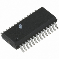
IC CTRLR DDR/PWM DUAL HE 28QSOP
Manufacturer
Fairchild Semiconductor
Specifications of FAN5236QSC
Applications
Controller, Mobile-Friendly DDR
Voltage - Input
5 ~ 24 V
Number Of Outputs
2
Voltage - Output
0.9 ~ 5 V
Operating Temperature
-10°C ~ 85°C
Mounting Type
Surface Mount
Package / Case
28-QSOP
Operating Temperature Range
- 10 C to + 85 C
Mounting Style
SMD/SMT
Lead Free Status / RoHS Status
Lead free / RoHS Compliant
Other names
FAN5236QSC_NL
FAN5236QSC_NL
FAN5236QSC_NL
Available stocks
Company
Part Number
Manufacturer
Quantity
Price

Part Number:
FAN5236QSC
Manufacturer:
FAIRCHILD/仙童
Quantity:
20 000
Company:
Part Number:
FAN5236QSCX
Manufacturer:
FAIRCHIL
Quantity:
17 500
Part Number:
FAN5236QSCX
Manufacturer:
FAIRCHILD/仙童
Quantity:
20 000


PRODUCT SPECIFICATION
Pin Definitions
Absolute Maximum Ratings
Absolute maximum ratings are the values beyond which the device may be damaged or have its useful life
impaired. Functional operation under these conditions is not implied.
Recommended Operating Conditions
Note 1: Industrial temperature range (–40 to + 85°C) may be special ordered from Fairchild. Please contact your authorized Fairchild
representative for more information.
4
Number
Parameter
VCC Supply Voltage:
VIN
BOOT, SW, ISNS, HDRV
BOOTx to SWx
All Other Pins
Junction Temperature (T
Storage Temperature
Lead Soldering Temperature, 10 seconds
Parameter
Supply Voltage VCC
Supply Voltage VIN
Ambient Temperature (T
Pin
14
15
16
18
28
REF2OUT
Pin Name
ILIM2 /
PG2 /
REF2
VCC
PG1
VIN
(continued)
Input Voltage. Normally connected to battery, providing voltage feed-forward to set the
amplitude of the internal oscillator ramp. When using the IC for 2-step conversion from 5V
input, connect through 100K to ground, which will set the appropriate ramp gain and
synchronize the channels 90˚ out of phase.
Power Good Flag. An open-drain output that will pull LOW when VSEN is outside of a
±10% range of the 0.9V reference.
Power Good 2. When not in DDR Mode: Open-drain output that pulls LOW when the
VOUT is out of regulation or in a fault condition
Reference Out 2. When in DDR Mode, provides a buffered output of REF2. Typically
used as the VDDQ/2 reference.
Current Limit 2. When not in DDR Mode, A resistor from this pin to GND sets the current
limit.
Reference for reg #2 when in DDR Mode. Typically set to VOUT1 / 2.
VCC. This pin powers the chip as well as the LDRV buffers. The IC starts to operate when
voltage on this pin exceeds 4.6V (UVLO rising) and shuts down when it drops below 4.3V
(UVLO falling).
A
J
)
)
Note 1
Conditions
Pin Function Description
Min.
4.75
Min.
–0.3
–10
–40
–65
Typ.
Typ.
5
VCC+0.3
Max.
Max.
150
150
300
5.25
6.5
6.5
27
33
24
85
REV. 1.1.9 7/12/04
Units
Units
FAN5236
°C
°C
°C
°C
V
V
V
V
V
V
V
Related parts for FAN5236QSC
Image
Part Number
Description
Manufacturer
Datasheet
Request
R

Part Number:
Description:
Manufacturer:
Fairchild Semiconductor
Datasheet:
Part Number:
Description:
Fairchild Semiconductor [IGBT MODULE]
Manufacturer:
Fairchild Semiconductor
Datasheet:

Part Number:
Description:
Discrete Semiconductor Modules
Manufacturer:
Fairchild Semiconductor
Part Number:
Description:
Discrete Semiconductor Modules
Manufacturer:
Fairchild Semiconductor
Part Number:
Description:
This N-Channel MOSFET is produced using Fairchild Semiconductor’s advanced Power Trench® process
Manufacturer:
Fairchild Semiconductor
Datasheet:
Part Number:
Description:
This N-Channel MOSFET is produced using Fairchild Semiconductor’s advanced Power Trench® process
Manufacturer:
Fairchild Semiconductor
Datasheet:
Part Number:
Description:
This N-Channel MOSFET is produced using Fairchild Semiconductor’s advanced PowerTrench® process
Manufacturer:
Fairchild Semiconductor
Datasheet:
Part Number:
Description:
This N-Channel MOSFET is produced using Fairchild Semiconductor’s advanced PowerTrench® process
Manufacturer:
Fairchild Semiconductor
Datasheet:
Part Number:
Description:
This N-Channel MOSFET is produced using Fairchild Semiconductor’s advanced Power Trench® process
Manufacturer:
Fairchild Semiconductor
Datasheet:
Part Number:
Description:
This N-Channel logic Level MOSFETs are produced using Fairchild Semiconductor‘s advanced Power Trench® process that has been special tailored to minimize the on-state resistance and yet maintain superior switching performance
Manufacturer:
Fairchild Semiconductor
Datasheet:
Part Number:
Description:
This N-Channel MOSFET is produced using Fairchild Semiconductor’s advanced Power Trench® process
Manufacturer:
Fairchild Semiconductor
Datasheet:
Part Number:
Description:
This N-Channel SyncFET™ is produced using Fairchild Semiconductor’s advanced PowerTrench® process
Manufacturer:
Fairchild Semiconductor
Datasheet:
Part Number:
Description:
This N-Channel SyncFET™ is produced using Fairchild Semiconductor’s advanced PowerTrench® process
Manufacturer:
Fairchild Semiconductor
Datasheet:
Part Number:
Description:
This N-Channel SyncFET™ is produced using Fairchild Semiconductor’s advanced PowerTrench® process
Manufacturer:
Fairchild Semiconductor
Datasheet:
Part Number:
Description:
This N-Channel logic Level MOSFETs are produced using Fairchild Semiconductor‘s advanced Power Trench® process that has been special tailored to minimize the on-state resistance and yet maintain superior switching performance
Manufacturer:
Fairchild Semiconductor
Datasheet: