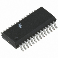
FAN5236QSC Fairchild Semiconductor, FAN5236QSC Datasheet - Page 16

FAN5236QSC
Manufacturer Part Number
FAN5236QSC
Description
IC CTRLR DDR/PWM DUAL HE 28QSOP
Manufacturer
Fairchild Semiconductor
Specifications of FAN5236QSC
Applications
Controller, Mobile-Friendly DDR
Voltage - Input
5 ~ 24 V
Number Of Outputs
2
Voltage - Output
0.9 ~ 5 V
Operating Temperature
-10°C ~ 85°C
Mounting Type
Surface Mount
Package / Case
28-QSOP
Operating Temperature Range
- 10 C to + 85 C
Mounting Style
SMD/SMT
Lead Free Status / RoHS Status
Lead free / RoHS Compliant
Other names
FAN5236QSC_NL
FAN5236QSC_NL
FAN5236QSC_NL
Available stocks
Company
Part Number
Manufacturer
Quantity
Price
Part Number:
FAN5236QSC
Manufacturer:
FAIRCHILD/仙童
Quantity:
20 000
Company:
Part Number:
FAN5236QSCX
Manufacturer:
FAIRCHIL
Quantity:
17 500
Part Number:
FAN5236QSCX
Manufacturer:
FAIRCHILD/仙童
Quantity:
20 000
PRODUCT SPECIFICATION
These losses are given by:
P
P
P
MOSFET. R
(T
Figure 15.
The driver’s impedance and C
period is controlled by the driver’s impedance and Q
Since most of t
constant current assumption for the driver to simplify the
calculation of t
16
UPPER
UPPER
COND
J
). t
P
P
C
SW
S
COND
is the upper MOSFET’s total losses, and P
ISS
V
V
= P
is the switching period (rise or fall time) and is t2+t3
are the switching and conduction losses for a given
V
DS
GS
V
I
TH
=
D
SP
= C
SW
Figure 16. Switching losses and Q
=
Figure 17. Drive Equivalent Circuit
DS(ON)
V
--------------------- -
GS
+ P
5V
DS
V
--------------
S
S
R
V
:
2
OUT
|| C
occurs when V
D
COND
IN
t1
I
C
is at the maximum junction temperature
GD
L
Q
ISS
GS
I
2 t
OUT
t2
2
S
SW
HDRV
Q
F
ISS
R
G(SW)
SW
GS
DS ON
C
determine t2 while t3’s
Q
= V
RSS
GD
t3
G
SP
R
we can use a
GATE
C
GS
C
t4
GD
C
ISS
G
SW
VIN
t5
and
GD
4.5V
(19b)
(19a)
.
Most MOSFET vendors specify Q
be determined as: Q
the the gate charge required to get the MOSFET to it’s
threshold (V
which can be as high as 20V in a typical portable applica-
tion. Care should also be taken to include the delivery of the
MOSFET’s gate power (P
dissipation required for the FAN5236:
where Q
Low-Side Losses
Q2, however, switches on or off with its parallel shottky
diode conducting, therefore V
proportional to V
and we can select Q2 based on R
Conduction losses for Q2 are given by:
where R
operating junction temperature and
Since D
produces a conservative result, further simplifying the
calculation.
The maximum power dissipation (P
the maximum allowable die temperature of the low-side
MOSFET, the
temperature rise:
be devoted to heat sinking (see FSC app note AN-1029 for
SO-8 MOSFET thermal information).
D
J-A
P
=
, depends primarily on the amount of PCB area that can
P
GATE
t
S
D MAX
V
--------------
P
V
=
COND
MIN
OUT
DS(ON)
G
IN
= Q
-------------------- -
I
Q
is the total gate charge to reach VCC.
DRIVER
G SW
TH
< 20% for portable computers, (1-D) 1
is the minimum duty cycle for the converter.
G
=
=
). For the high-side MOSFET, V
is the R
J-A
T
------------------------------------------------- -
VCC F
DS
1 D
J MAX
, and the maximum allowable ambient
–
G(SW)
, Q2’s switching losses are negligible
---------------------------------------------------- -
---------------------------------------------- -
R
DS(ON)
DRIVER
J A
VCC V
SW
–
GATE
I
–
= Q
Q
OUT
T
A MAX
G SW
GD
DS
2
of the MOSFET at the highest
–
+
) in calculating the power
R
DS(ON)
+ Q
R
SP
GATE
GD
0.5V. Since P
DS ON
D(MAX)
GS
and Q
– Q
only.
) is a function of
REV. 1.1.9 7/12/04
TH
GS
. Q
where Q
DS
SW
G(SW)
= VIN,
is
FAN5236
(20)
(22)
TH
(23)
(21)
can
is


