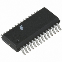
FAN5236QSC Fairchild Semiconductor, FAN5236QSC Datasheet - Page 12

FAN5236QSC
Manufacturer Part Number
FAN5236QSC
Description
IC CTRLR DDR/PWM DUAL HE 28QSOP
Manufacturer
Fairchild Semiconductor
Specifications of FAN5236QSC
Applications
Controller, Mobile-Friendly DDR
Voltage - Input
5 ~ 24 V
Number Of Outputs
2
Voltage - Output
0.9 ~ 5 V
Operating Temperature
-10°C ~ 85°C
Mounting Type
Surface Mount
Package / Case
28-QSOP
Operating Temperature Range
- 10 C to + 85 C
Mounting Style
SMD/SMT
Lead Free Status / RoHS Status
Lead free / RoHS Compliant
Other names
FAN5236QSC_NL
FAN5236QSC_NL
FAN5236QSC_NL
Available stocks
Company
Part Number
Manufacturer
Quantity
Price
Part Number:
FAN5236QSC
Manufacturer:
FAIRCHILD/仙童
Quantity:
20 000
Company:
Part Number:
FAN5236QSCX
Manufacturer:
FAIRCHIL
Quantity:
17 500
Part Number:
FAN5236QSCX
Manufacturer:
FAIRCHILD/仙童
Quantity:
20 000
PRODUCT SPECIFICATION
Current Processing Section
The following discussion refers to Figure 11.
The current through R
shortly after Q2 is turned on. That current is held, and
summed with the output of the error amplifier. This effec-
tively creates a current mode control loop. The resistor con-
nected to ISNSx pin (R
feedback loop. For stable operation, the voltage induced by
the current feedback at the PWM comparator input should be
set to 30% of the ramp amplitude at maximum load currrent
and line voltage. The following expression estimates the
recommended value of R
mum load current (I
MOSFET’s R
R
Setting the Current Limit
A ratio of ISNS is also compared to the current established
when a 0.9 V internal reference drives the ILIM pin:
Since the tolerance on the current limit is largely dependent
on the ratio of the external resistors it is fairly accurate if the
voltage drop on the Switching Node side of R
accurate representation of the load current. When using the
MOSFET as the sensing element, the variation of R
causes proportional variation in the ISNS. This value not
only varies from device to device, but also has a typical junc-
tion temperature coefficient of about 0.4% / °C (consult the
MOSFET datasheet for actual values), so the actual current
limit set point will decrease propotional to increasing
MOSFET die temperature. A factor of 1.6 in the current
limit setpoint should compensate for all MOSFET R
variations, assuming the MOSFET’s heat sinking will keep
its operating die temperature below 125°C.
12
SENSE
R
R
SENSE
SENSE MIN
Figure 12. Improving current sensing accuracy
R
ILIM
must, however, be kept higher than:
=
=
DS(ON)
I
---------------------------------------------------------------------------- - 100
LOAD MAX
--------------- -
I
LIMIT
11.2
0.30 0.125 V
=
LOAD(MAX)
I
---------------------------------------------------------- - 100
:
LOAD MAX
SENSE
ISNS
SENSE
LDRV
PGND
--------------------------------------- -
100
SENSE
R
150 A
R
+
resistor (ISNS) is sampled
DS ON
R
) sets the gain in the current
DS ON
SENSE
R
) and the value of the
as a function of the maxi-
SENSE
IN MAX
R
DS ON
Q2
4.1K
–
–
SENSE
DS(ON)
is an
DS(ON)
(4a)
(4b)
(5)
More accurate sensing can be achieved by using a resistor
(R1) instead of the R
12. This approach causes higher losses, but yields greater
accuracy in both V
(e.g. 10m ) resistor.
Current limit (I
allow inductor current to rise in response to an output load
transient. Typically, a factor of 1.2 is sufficient. In addition,
since I
multiply I
use 25%). For example, in Figure 5 the target for I
would be:
Duty Cycle Clamp
During severe load increase, the error amplifier output can
go to its upper limit pushing a duty cycle to almost 100% for
significant amount of time. This could cause a large increase
of the inductor current and lead to a long recovery from a
transient, over-current condition, or even to a failure espe-
cially at high input voltages. To prevent this, the output of
the error amplifier is clamped to a fixed value after two clock
cycles if severe output voltage excursion is detected, limiting
the maximum duty cycle to
This circuit is designed to not interfere with normal PWM
operation. When FPWM is grounded, the duty cycle clamp
is disabled and the maximum duty cycle is 87%.
Gate Driver section
The Adaptive gate control logic translates the internal PWM
control signal into the MOSFET gate drive signals providing
necessary amplification, level shifting and shoot-through
protection. Also, it has functions that help optimize the IC
performance over a wide range of operating conditions.
Since MOSFET switching time can vary dramatically from
type to type and with the input voltage, the gate control logic
provides adaptive dead time by monitoring the gate-to-
source voltages of both upper and lower MOSFETs.
The lower MOSFET drive is not turned on until the gate-to-
source voltage of the upper MOSFET has decreased to less
than approximately 1 volt. Similarly, the upper MOSFET is
not turned on until the gate-to-source voltage of the lower
MOSFET has decreased to less than approximately 1 volt.
This allows a wide variety of upper and lower MOSFETs to
be used without a concern for simultaneous conduction, or
shoot-through.
There must be a low-resistance, low-inductance path
between the driver pin and the MOSFET gate for the adap-
tive dead-time circuit to work properly. Any delay along that
path will subtract from the delay generated by the adaptive
dead-time circit and shoot-through may occur.
I
LIMIT
DC
LIMIT
MAX
LOAD(MAX)
> 1.2 1.25 1.6 6A 14A
is a peak current cut-off value, we will need to
=
LIMIT
V
--------------
V
OUT
DROOP
IN
) should be set sufficiently high as to
DS(ON)
by the inductor ripple current (we’ll
+
---------
V
2.4
and I
IN
of the FET as shown in Figure
LIMIT
. R1 is a low value
REV. 1.1.9 7/12/04
LIMIT
FAN5236
(6)


