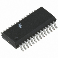
FAN5236QSC Fairchild Semiconductor, FAN5236QSC Datasheet - Page 3

FAN5236QSC
Manufacturer Part Number
FAN5236QSC
Description
IC CTRLR DDR/PWM DUAL HE 28QSOP
Manufacturer
Fairchild Semiconductor
Specifications of FAN5236QSC
Applications
Controller, Mobile-Friendly DDR
Voltage - Input
5 ~ 24 V
Number Of Outputs
2
Voltage - Output
0.9 ~ 5 V
Operating Temperature
-10°C ~ 85°C
Mounting Type
Surface Mount
Package / Case
28-QSOP
Operating Temperature Range
- 10 C to + 85 C
Mounting Style
SMD/SMT
Lead Free Status / RoHS Status
Lead free / RoHS Compliant
Other names
FAN5236QSC_NL
FAN5236QSC_NL
FAN5236QSC_NL
Available stocks
Company
Part Number
Manufacturer
Quantity
Price
Part Number:
FAN5236QSC
Manufacturer:
FAIRCHILD/仙童
Quantity:
20 000
Company:
Part Number:
FAN5236QSCX
Manufacturer:
FAIRCHIL
Quantity:
17 500
Part Number:
FAN5236QSCX
Manufacturer:
FAIRCHILD/仙童
Quantity:
20 000
FAN5236
Pin Configurations
Pin Definitions
REV. 1.1.9 7/12/04
Number
Pin
27
26
25
24
23
22
21
20
10
19
11
12
17
13
1
2
3
4
5
6
7
8
9
Pin Name
FPWM1
FPWM2
PGND1
PGND2
HDRV1
BOOT1
BOOT2
LDRV1
LDRV2
VSEN1
VSEN2
AGND
ISNS1
ISNS2
ILIM1
SW1
SW2
DDR
EN1
EN2
SS1
SS2
Analog Ground. This is the signal ground reference for the IC. All voltage levels are
measured with respect to this pin.
Low-Side Drive. The low-side (lower) MOSFET driver output. Connect to gate of low-side
MOSFET.
Power Ground. The return for the low-side MOSFET driver. Connect to source of low-
side MOSFET.
Switching node. Return for the high-side MOSFET driver and a current sense input.
Connect to source of high-side MOSFET and low-side MOSFET drain.
High-Side Drive. High-side (upper) MOSFET driver output. Connect to gate of high-side
MOSFET.
BOOT. Positive supply for the upper MOSFET driver. Connect as shown in Figure 3.
Current Sense input. Monitors the voltage drop across the lower MOSFET or external
sense resistor for current feedback.
Enable . Enables operation when pulled to logic high. Toggling EN will also reset the
regulator after a latched fault condition. These are CMOS inputs whose state is
indeterminate if left open.
Forced PWM mode. When logic low, inhibits the regulator from entering hysteretic mode.
Otherwise tie to VOUT. The regulator uses VOUT on this pin to ensure a smooth
transition from Hysteretic mode to PWM mode. When VOUT is expected to exceed VCC,
tie to VCC.
Output Voltage Sense. The feedback from the outputs. Used for regulation as well as
PG, under-voltage and over-voltage protection and monitoring.
Current Limit 1. A resistor from this pin to GND sets the current limit.
Soft Start. A capacitor from this pin to GND programs the slew rate of the converter
during initialization. During initialization, this pin is charged with a 5 A current source.
DDR Mode Control. High = DDR mode. Low = 2 separate regulators operating 180° out
of phase.
FPWM1
PGND1
HDRV1
BOOT1
LDRV1
VSEN1
AGND
ISNS1
ILIM1
SW1
DDR
EN1
SS1
VIN
QSOP-28 or TSSOP-28
1
2
3
4
5
6
7
8
9
10
11
12
13
14
JA
FAN5236
= 90 C/W
Pin Function Description
28
27
26
25
24
23
22
21
20
19
18
17
16
15
VCC
LDRV2
PGND2
SW2
HDRV2
BOOT2
ISNS2
EN2
FPWM2
VSEN2
ILIM2/REF2
SS2
PG2/REF2OUT
PG1
PRODUCT SPECIFICATION
3


