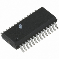
FAN5236QSC Fairchild Semiconductor, FAN5236QSC Datasheet - Page 10

FAN5236QSC
Manufacturer Part Number
FAN5236QSC
Description
IC CTRLR DDR/PWM DUAL HE 28QSOP
Manufacturer
Fairchild Semiconductor
Specifications of FAN5236QSC
Applications
Controller, Mobile-Friendly DDR
Voltage - Input
5 ~ 24 V
Number Of Outputs
2
Voltage - Output
0.9 ~ 5 V
Operating Temperature
-10°C ~ 85°C
Mounting Type
Surface Mount
Package / Case
28-QSOP
Operating Temperature Range
- 10 C to + 85 C
Mounting Style
SMD/SMT
Lead Free Status / RoHS Status
Lead free / RoHS Compliant
Other names
FAN5236QSC_NL
FAN5236QSC_NL
FAN5236QSC_NL
Available stocks
Company
Part Number
Manufacturer
Quantity
Price
Part Number:
FAN5236QSC
Manufacturer:
FAIRCHILD/仙童
Quantity:
20 000
Company:
Part Number:
FAN5236QSCX
Manufacturer:
FAIRCHIL
Quantity:
17 500
Part Number:
FAN5236QSCX
Manufacturer:
FAIRCHILD/仙童
Quantity:
20 000
PRODUCT SPECIFICATION
These problems are nicely solved by delaying the 2
verter’s clock by 90° as shown in Figure 9. In this way, all
switching transitions in one converter take place far away
from the decision points of the other converter.
Initialization and Soft Start
Assuming EN is high, FAN5236 is initialized when VCC
exceeds the rising UVLO threshold. Should VCC drop
below the UVLO threshold, an internal Power-On Reset
function disables the chip.
The voltage at the positive input of the error amplifier is lim-
ited by the voltage at the SS pin which is charged with a 5 A
current source. Once C
output voltage will be in regulation. The time it takes SS to
reach 0.9V is:
where T
10
Figure 8. Noise-susceptible In-Phase operation for DDR2
V
V
V
V
V
V
CORE
CORE
CORE
CORE
T
I
VDDQ
VDDQ
I
0.9
L
VTT
VTT
L
CLK
CLK
0
0
0.9
=
Figure 9. Optimal 90° phasing for DDR2
0.9 C
---------------------- -
is in seconds if C
5
SS
SS
has charged to VREF (0.9V) the
SS
is in F.
Figure 10. Transitioning between PWM and Hysteretic Mode
1
PWM Mode
2
1
nd
2
Hysteretic Mode
Hy y
3
y
ys
con-
(1)
3
4
de
4
When SS reaches 1.5V, the Power Good outputs are enabled
and hysteretic mode is allowed. The converter is forced into
PWM mode during soft start.
Operation Mode Control
The mode-control circuit changes the converter’s mode of
operation from PWM to Hysteretic and visa versa, based on
the voltage polarity of the SW node when the lower MOS-
FET is conducting and just before the upper MOSFET turns
on. For continuous inductor current, the SW node is negative
when the lower MOSFET is conducting and the converters
operate in fixed-frequency PWM mode as shown in Figure
10. This mode of operation achieves high efficiency at nomi-
nal load. When the load current decreases to the point where
the inductor current flows through the lower MOSFET in the
‘reverse’ direction, the SW node becomes positive, and the
mode is changed to hysteretic, which achieves higher effi-
ciency at low currents by decreasing the effective switching
frequency.
To prevent accidental mode change or "mode chatter" the
transition from PWM to Hysteretic mode occurs when the
SW node is positive for eight consecutive clock cycles (see
Figure 10). The polarity of the SW node is sampled at the
end of the lower MOSFET’s conduction time. At the transi-
tion between PWM and hysteretic mode both the upper and
lower MOSFETs are turned off. The phase node will ‘ring’
based on the output inductor and the parasitic capacitance on
the phase node and settle out at the value of the output volt-
age.
The boundary value of inductor current, where current
becomes discontinuous, can be estimated by the following
expression.
5
I
LOAD DIS
6
5
7
=
8
--------------------------------------------------
V
6
2F
IN
Hysteretic Mode
SW
–
y
ste e e
V
L
OUT
OUT
V
V
7
IN
OUT
8
REV. 1.1.9 7/12/04
PWM Mode
FAN5236
(2)


