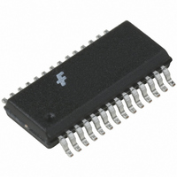
FAN5236QSC Fairchild Semiconductor, FAN5236QSC Datasheet - Page 15

FAN5236QSC
Manufacturer Part Number
FAN5236QSC
Description
IC CTRLR DDR/PWM DUAL HE 28QSOP
Manufacturer
Fairchild Semiconductor
Specifications of FAN5236QSC
Applications
Controller, Mobile-Friendly DDR
Voltage - Input
5 ~ 24 V
Number Of Outputs
2
Voltage - Output
0.9 ~ 5 V
Operating Temperature
-10°C ~ 85°C
Mounting Type
Surface Mount
Package / Case
28-QSOP
Operating Temperature Range
- 10 C to + 85 C
Mounting Style
SMD/SMT
Lead Free Status / RoHS Status
Lead free / RoHS Compliant
Other names
FAN5236QSC_NL
FAN5236QSC_NL
FAN5236QSC_NL
Available stocks
Company
Part Number
Manufacturer
Quantity
Price
Part Number:
FAN5236QSC
Manufacturer:
FAIRCHILD/仙童
Quantity:
20 000
Company:
Part Number:
FAN5236QSCX
Manufacturer:
FAIRCHIL
Quantity:
17 500
Part Number:
FAN5236QSCX
Manufacturer:
FAIRCHILD/仙童
Quantity:
20 000
FAN5236
Output Capacitor Selection
The output capacitor serves two major functions in a switch-
ing power supply. Along with the inductor it filters the
sequence of pulses produced by the switcher, and it supplies
the load transient currents. The output capacitor require-
ments are usually dictated by ESR, Inductor ripple current
( I) and the allowable ripple voltage ( V).
In addition, the capacitor’s ESR must be low enough to allow
the converter to stay in regulation during a load step. The
ripple voltage due to ESR for the converter in Figure 5 is
120mV P-P. Some additional ripple will appear due to the
capacitance value itself:
which is only about 1.5mV for the converter in Figure 5 and
can be ignored.
The capacitor must also be rated to withstand the RMS
current which is approximately 0.3 X ( I), or about 400mA
for the converter in Figure 5. High frequency decoupling
capacitors should be placed as close to the loads as
physically possible.
Input Capacitor Selection
The input capacitor should be selected by its ripple current
rating.
Two-Stage Converter Case
In DDR mode (Figure 4), the VTT power input is powered
by the VDDQ output, therefore all of the input capacitor rip-
ple current is produced by the VDDQ converter. A conserva-
tive estimate of the output
current required for the 2.5V regulator is:
As an example, if average I
1A, I
age is 16V, RMS input ripple current will be:
where D is the duty cycle of the PWM1 converter:
REV. 1.1.9 7/12/04
VDDQ
I
D
I
ESR
RMS
REG1
V
V
--------------
=
V
OUT
current will be about 3.5A. If average input volt-
=
IN
=
---------------------------------------- -
C
------- -
I
OUT
V
OUT MAX
I
I
VDDQ
=
2.5
------ -
16
8 F
I
+
I
----------- -
VTT
2
SW
D D
VDDQ
–
2
is 3A, and average I
VTT
(13)
(14)
(15)
(16)
is
therefore:
Dual Converter 180° phased
In Dual mode (Figure 5), both converters contribute to the
capacitor input ripple current. With each converter operating
180° out of phase, the RMS currents add in the following
fashion:
which for the dual 3A converters of Figure 5, calculates to:
Power MOSFET Selection
Losses in a MOSFET are the sum of its switching (P
conduction (P
In typical applications, the FAN5236 converter’s output volt-
age is low with respect to its input voltage, therefore the
Lower MOSFET (Q2) is conducting the full load current for
most of the cycle. Q2 should therefore be selected to mini-
mize conduction losses, thereby selecting a MOSFET with
low R
In contrast, the high-side MOSFET (Q1) has a much shorter
duty cycle, and it’s conduction loss will therefore have less
of an impact. Q1, however, sees most of the switching losses,
so Q1’s primary selection criteria should be gate charge.
High-Side Losses:
Figure 15 shows a MOSFET’s switching interval, with the
upper graph being the voltage and current on the Drain to
Source and the lower graph detailing V
constant current charging the gate. The x-axis therefore is
also representative of gate charge (Q
and it controls t1, t2, and t4 timing. C
from the gate driver during t3 (as V
charge (Q
specified or can be derived from MOSFET datasheets.
Assuming switching losses are about the same for both the
rising edge and falling edge, Q1’s switching losses, occur
during the shaded time when the MOSFET has voltage
across it and current through it.
I
I
I
I
RMS
RMS
RMS
RMS
DS(ON)
G
=
=
=
=
) parameters on the lower graph are either
.
3.5
1.4A
COND
I
RMS 1
I
1
2.5
------ -
16
2
) losses.
D
–
2
1
+
–
2.5
------ -
16
I
D
RMS 2
1
2
2
+
=
2
1.49A
I
or
2
PRODUCT SPECIFICATION
2
DS
G
D
GD
) . C
2
is falling). The gate
GS
–
receives the current
D
vs. time with a
ISS
2
2
= C
GD
SW
+ C
(18a)
(18b)
(17)
) and
GS
15
,


