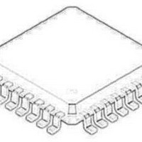
NCP5331FTR2G ON Semiconductor, NCP5331FTR2G Datasheet - Page 32

NCP5331FTR2G
Manufacturer Part Number
NCP5331FTR2G
Description
IC CTLR PWM 2PH W/DRVRS 32-LQFP
Manufacturer
ON Semiconductor
Datasheet
1.NCP5331FTR2G.pdf
(36 pages)
Specifications of NCP5331FTR2G
Applications
Controller, AMD Athlon™
Voltage - Input
9 ~ 14 V
Number Of Outputs
2
Voltage - Output
5V
Operating Temperature
0°C ~ 70°C
Mounting Type
Surface Mount
Package / Case
32-LQFP
Mounting Style
SMD/SMT
Lead Free Status / RoHS Status
Lead free / RoHS Compliant
Other names
NCP5331FTR2G
NCP5331FTR2GOSTR
NCP5331FTR2GOSTR
Available stocks
Company
Part Number
Manufacturer
Quantity
Price
Company:
Part Number:
NCP5331FTR2G
Manufacturer:
ON Semiconductor
Quantity:
10 000
Part Number:
NCP5331FTR2G
Manufacturer:
ON/安森美
Quantity:
20 000
2. Output Inductor Selection
according to Equation 3 with 20% inductor ripple current
( = 0.15).
from Micrometals: 23.0 nH/N
the Micrometals catalog, at 26 A (per phase) the
permeability of this core will be approximately 88% of the
permeability at 0 A. Therefore, at 0 A we must achieve at
least 673 nH/0.88 or 765 nH. Using 6 turns of #16 AWG
bifilar (2 mW/ft) will produce 828 nH.
resistances for subsequent calculations.
inductor is “hot” due to the load current and the ambient
temperature is high. Assuming a 50 C temperature rise of
the inductor at full−load and a 35 C ambient temperature
rise we can calculate
R L,MAX + 0.965 mW @ [1 ) 0.39% °C @ (50°C ) 35°C)]
the saturation characteristic of the core material.
will satisfy the design goal with the minimum number of
output capacitors and the full load output inductance.
V OUT,P−P + (ESR per cap
number of output capacitors is used. More output capacitors
will probably be required to satisfy the transient
requirement, which will result in a lower ripple voltage.
3. Input Capacitor Selection
the converter at full−load.
R L + 6 turns @ 2.5 cm turn @ 0.03218 ft cm @ 2 mW ft
Calculate the minimum output inductance at I
To minimize core losses, we choose the T50 8B/90 core
We will need the nominal and worst case inductor
The inductor resistance will be maximized when the
The output inductance at full−load will be reduced due to
Next, use Equation 4 to insure the output voltage ripple
So, the ripple requirement will be satisfied if the minimum
Use Equation 5 to determine the average input current to
+ (19 mW 6) @ {(12 V * 2 @ 1.163 V)
+ 20 mV
I IN,AVG + I O,MAX @ D h
+ 0.965 mW
Lo 52 A + 0.88
@ (1.163 V 12 V) (729 nH @ 200 kHz)}
@ {(V IN * #Phases @ V CORE ) @ D
+ 1.28 mW
Lo MIN +
+ 52 A @ (1.163 V 12 V) 0.80 + 6.30 A
+
+ 673 nH
(a @ I O,MAX @ V IN @ f SW )
(0.15 @ 52 A @ 12 V @ 200 kHz)
(V IN * V OUT ) @ V OUT
(12 V * 1.163 V) @ 1.163 V
828 nH + 729 nH at full load
2
N OUT,MIN )
, 2.50 cm/turn. According to
(Lo 52 A @ f SW )}
http://onsemi.com
O,MAX
(3)
(4)
(5)
NCP5331
32
inductance value of 729 nH.
current at full−load is as follows. (Note: D = 1.163 V/12 V
= 0.097.)
I CIN,RMS + [2D @ (I C,MIN 2 ) I C,MIN @ DI C,IN
board space by using higher−rated/more costly capacitors
or saving cost by using more lower−rated/less costly
capacitors. To save cost, we choose the MBZ series
capacitors by Rubycon. Part number 16MBZ1500M10X20:
1500 mF, 16 V, 2.55 A
will require N
for a cost sensitive design or 6 capacitors for a conservative
design.
4. Input Inductor Selection
limit the input current slew rate to less than 0.5 A/ms during
a load transient from 0 to 52 A. A conservative value will be
calculated assuming the minimum number of output
capacitors (N
case ESR values for both the input and output capacitors,
and a maximum duty cycle at the maximum DAC setting
with 25 mV of no−load AVP.
Next, use Equation 6 to Equation 10 with the full−load
For the two−phase converter, the input capacitor(s) rms
At this point, the designer must decide between saving
For the Claw Hammper CPU, the input inductor must
D MAX + (1.550 V ) 25 mV AVP ) 10.8 V IN + 0.146
DI Lo + (V IN * V OUT ) @ D (Lo @ f SW )
I C,MAX + I Lo,MAX h * I IN,AVG
I C,MIN + I Lo,MIN h * I IN,AVG
I Lo,MAX + I O,MAX 2 ) DI Lo 2
I Lo,MIN + I O,MAX 2 * DI Lo 2
+ [0.19 @ (21.7 2 ) 21.7 @ 9.0 ) 9.0 2 3)
+ 12.9 A RMS
+ (12 V * 1.163 V) @
+ 7.20 App
OUT
IN
) DI C,IN 2 3) ) I IN,AVG 2 @ (1 * 2D)] 1 2
) 6.30 2 @ (1 * 0.19)] 1 2
= 12.8 A/2.55 A = 5 capacitors on the input
+ 22.4 A 0.80 * 6.30 A + 21.7 A
+ 29.6 A 0.80 * 6.30 A + 30.7 A
= 6), five input capacitors (N
+ 52 A 2 * 7.20 App 2 + 22.4 A
+ 52 A 2 ) 7.20 App 2 + 29.6 A
RMS
, 13 mW, 10 20 mm. This design
(729 nH @ 200 kHz)
(1.163 V 12 V)
IN
= 5), worst
(10)
(11)
(8)
(9)
(6)
(7)


