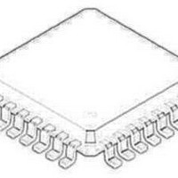
NCP5331FTR2G ON Semiconductor, NCP5331FTR2G Datasheet - Page 29

NCP5331FTR2G
Manufacturer Part Number
NCP5331FTR2G
Description
IC CTLR PWM 2PH W/DRVRS 32-LQFP
Manufacturer
ON Semiconductor
Datasheet
1.NCP5331FTR2G.pdf
(36 pages)
Specifications of NCP5331FTR2G
Applications
Controller, AMD Athlon™
Voltage - Input
9 ~ 14 V
Number Of Outputs
2
Voltage - Output
5V
Operating Temperature
0°C ~ 70°C
Mounting Type
Surface Mount
Package / Case
32-LQFP
Mounting Style
SMD/SMT
Lead Free Status / RoHS Status
Lead free / RoHS Compliant
Other names
NCP5331FTR2G
NCP5331FTR2GOSTR
NCP5331FTR2GOSTR
Available stocks
Company
Part Number
Manufacturer
Quantity
Price
Company:
Part Number:
NCP5331FTR2G
Manufacturer:
ON Semiconductor
Quantity:
10 000
Part Number:
NCP5331FTR2G
Manufacturer:
ON/安森美
Quantity:
20 000
NOTE:
NOTE:
Figure 36. V
Figure 35. V
The RC time constant of the current sense network is
too short (fast); V
The RC time constant of the current sense network is
too long (slow); V
DRP
DRP
tuning, RC Time Too Short
Tuning, RC Time Too Long
DRP
DRP
L1
I
L2
I
and V
MAX
MAX
and V
/2
/2
R
R
CORE
S1
S2
CORE
C
C
both overshoot.
S1
S2
respond too slowly.
Figure 34. AVP Circuitry at Full−Load
CS1
CS2
CS
REF
+
−
+
−
G
G
http://onsemi.com
VDRP
VDRP
NCP5331
V
CORE
V
I
MAX
29
DRP
= VID − (I
I
I
DRP
FBK
7. Current Sensing
network (RSx, CSx) to satisfy
network (RSx, CSx) to satisfy
CSx. After the converter is constructed, the value of RSx
(and/or LSx) should be fine−tuned in the lab by observing
the V
the RSx CSx network to provide a “square−wave” at the
V
overshoot as shown in Figures 34 − 36.
= VID +
NOTE:
R
DRP
COMP
For inductive current sensing, choose the current sense
For resistive current sensing, choose the current sense
This will provide an adequate starting point for RSx and
L
I
= I
DRP
= I
DRP
R
G
DRP
MAX
output pin with maximum rise time and minimal
DRP
DRP
VDRP
Figure 37. V
Error
Amp
The RC time constant of the current sense network is
optimal; V
quickly without overshooting.
− IBIAS
signal during a step change in load current. Tune
− IBIAS
V
R
RSx @ CSx + Lo (R L ) R PCB )
+
−
FB
L
RSx @ CSx + Lo (R sense )
= VID
G
VFB
VDRP
DRP
VFB
VID Setting
IBIAS
DRP
) w R
R
I
/R
and V
FBK
+ −
F1
DRP
VFB
Tuning, RC Time Optimal
F1
CORE
V
CORE
respond to the load current
(32)
(33)


