NCP5331FTR2G ON Semiconductor, NCP5331FTR2G Datasheet - Page 14
NCP5331FTR2G
Manufacturer Part Number
NCP5331FTR2G
Description
IC CTLR PWM 2PH W/DRVRS 32-LQFP
Manufacturer
ON Semiconductor
Datasheet
1.NCP5331FTR2G.pdf
(36 pages)
Specifications of NCP5331FTR2G
Applications
Controller, AMD Athlon™
Voltage - Input
9 ~ 14 V
Number Of Outputs
2
Voltage - Output
5V
Operating Temperature
0°C ~ 70°C
Mounting Type
Surface Mount
Package / Case
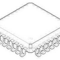
32-LQFP
Mounting Style
SMD/SMT
Lead Free Status / RoHS Status
Lead free / RoHS Compliant
Other names
NCP5331FTR2G
NCP5331FTR2GOSTR
NCP5331FTR2GOSTR
Available stocks
Company
Part Number
Manufacturer
Quantity
Price
Company:

Part Number:
NCP5331FTR2G
Manufacturer:
ON Semiconductor
Quantity:
10 000
Part Number:
NCP5331FTR2G
Manufacturer:
ON/安森美
Quantity:
20 000


Overview
topology to meet requirements of low voltage, high current
loads with fast transient requirements. Transient response
has been improved and voltage jitter virtually eliminated by
including an internal PWM ramp, connecting fast−feedback
from V
precise routing and grounding inside the controller.
Advanced features such as adjustable power−good delay,
programmable overcurrent shutdown time, superior
overvoltage protection (OVP), and differential remote
voltage sensing make it easy to obtain AMD certification.
An innovative overvoltage protection (OVP) scheme
safeguards the CPU during extreme situations including
power up with a shorted upper MOSFET, shorting of an
upper MOSFET during normal operation, and loss of the
voltage feedback signal, COREFB+. The NCP5331
provides a “fully integrated solution” to simplify design,
minimize circuit board area, and reduce overall system cost.
single−phase converter are current sharing and increased
apparent output frequency. Current sharing allows the
designer to use less inductance in each phase than would be
required in a single−phase converter. The smaller inductor
produces larger ripple currents but the total per phase power
dissipation is reduced because the rms current is lower.
Transient response is improved because the control loop will
measure and adjust the current faster in a smaller output
inductor. Increased apparent output frequency is desirable
because the off−time and the ripple voltage of the two−phase
converter will be less than that of a single−phase converter.
Fixed Frequency Multiphase Control
connected in parallel and are switched on at different times.
This reduces output current from the individual converters
and increases the apparent ripple frequency. Because several
The NCP5331 dc/dc controller utilizes an Enhanced V
Two advantages of a multiphase converter over a
In a multiphase converter, multiple converters are
CORE
Figure 14. Enhanced V
directly to the internal PWM comparator, and
SWNODE
Lx
2
(V
Control Employing Resistive Current Sensing and Additional Internal Ramp
CORE
V
OUT
RLx
)
RSx
APPLICATIONS INFORMATION
+
CSx
x = 1 or 2
CS
V
V
COMP
http://onsemi.com
FFB
FB
REF
NCP5331
DAC
2
Out
“Fast−Feedback”
14
Connection
+
−
converters are connected in parallel, output current can ramp
up or down faster than a single converter (with the same
value output inductor) and heat is spread among multiple
components.
frequency, Enhanced V
currents in individual phases. Each phase is delayed 180
from the previous phase. Normally, GHx (x = 1 or 2)
transitions to a high voltage at the beginning of each
oscillator cycle. Inductor current ramps up until the
combination of the current sense signal, the internal ramp
and the output voltage ripple trip the PWM comparator and
bring GHx low. Once GHx goes low, it will remain low until
the beginning of the next oscillator cycle. While GHx is
high, the Enhanced V
variations (i.e. the upper gate on−time will be increased or
reduced as required). On the other hand, once GHx is low,
the loop can not respond until the beginning of the next
PWM cycle. Therefore, constant frequency Enhanced V
will typically respond to disturbances within the off−time of
the converter.
output current in each phase. An additional input, CSx (x =
1 or 2), for inductor current information has been added to the
V
inductor current is measured differentially across RS,
amplified by CSA and summed with the Channel Startup
Offset, the Internal Ramp, and the Output Voltage at the
noninverting input of the PWM comparator. The purpose of
the Internal Ramp is to compensate for propagation delays in
the NCP5331. This provides greater design flexibility by
allowing smaller external ramps, lower minimum pulse
widths, higher frequency operation, and PWM duty cycles
above 50% without external slope compensation. As the sum
of the inductor current and the internal ramp increase, the
voltage on the positive pin of the PWM comparator rises and
terminates the PWM cycle. If the inductor starts a cycle
CSA
Internal Ramp
2
The NCP5331 controller uses a two−phase, fixed
The Enhanced V
loop for each phase as shown in Figure 14. The triangular
−
+
COn
Error
Amp
Start−Up
Channel
Offset
− +
2
architecture measures and adjusts the
2
2
loop will respond to line and load
architecture to measure and control
+
−
COMP
PWM
To F/F
Reset
2
Related parts for NCP5331FTR2G
Image
Part Number
Description
Manufacturer
Datasheet
Request
R

Part Number:
Description:
Two-Phase PWM Controller with Integrated Gate Drivers
Manufacturer:
ON Semiconductor
Datasheet:
Part Number:
Description:
ON Semiconductor [VOLTAGE REGULATOR]
Manufacturer:
ON Semiconductor
Datasheet:
Part Number:
Description:
357-036-542-201 CARDEDGE 36POS DL .156 BLK LOPRO
Manufacturer:
ON Semiconductor
Datasheet:
Part Number:
Description:
357-036-542-201 CARDEDGE 36POS DL .156 BLK LOPRO
Manufacturer:
ON Semiconductor
Datasheet:
Part Number:
Description:
357-036-542-201 CARDEDGE 36POS DL .156 BLK LOPRO
Manufacturer:
ON Semiconductor
Datasheet:
Part Number:
Description:
357-036-542-201 CARDEDGE 36POS DL .156 BLK LOPRO
Manufacturer:
ON Semiconductor
Datasheet:
Part Number:
Description:
357-036-542-201 CARDEDGE 36POS DL .156 BLK LOPRO
Manufacturer:
ON Semiconductor
Datasheet:
Part Number:
Description:
357-036-542-201 CARDEDGE 36POS DL .156 BLK LOPRO
Manufacturer:
ON Semiconductor
Datasheet:
Part Number:
Description:
357-036-542-201 CARDEDGE 36POS DL .156 BLK LOPRO
Manufacturer:
ON Semiconductor
Datasheet:
Part Number:
Description:
357-036-542-201 CARDEDGE 36POS DL .156 BLK LOPRO
Manufacturer:
ON Semiconductor
Datasheet:
Part Number:
Description:
357-036-542-201 CARDEDGE 36POS DL .156 BLK LOPRO
Manufacturer:
ON Semiconductor
Datasheet:
Part Number:
Description:
357-036-542-201 CARDEDGE 36POS DL .156 BLK LOPRO
Manufacturer:
ON Semiconductor
Datasheet:
Part Number:
Description:
Manufacturer:
ON Semiconductor
Datasheet:
Part Number:
Description:
Manufacturer:
ON Semiconductor
Datasheet: