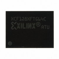
XCF128XFTG64C Xilinx Inc, XCF128XFTG64C Datasheet - Page 87

XCF128XFTG64C
Manufacturer Part Number
XCF128XFTG64C
Description
IC PROM SRL 128M GATE 64-FTBGA
Manufacturer
Xilinx Inc
Datasheet
1.XCF128XFTG64C.pdf
(88 pages)
Specifications of XCF128XFTG64C
Memory Size
128Mb
Programmable Type
In System Programmable
Voltage - Supply
1.7 V ~ 2 V
Operating Temperature
-40°C ~ 85°C
Package / Case
64-TBGA
Access Time
85ns
Supply Voltage Range
1.7V To 2V
Memory Case Style
FTBGA
No. Of Pins
64
Operating Temperature Range
-40°C To +85°C
Svhc
No SVHC (15-Dec-2010)
Package /
RoHS Compliant
Lead Free Status / RoHS Status
Lead free / RoHS Compliant
Other names
122-1578
Available stocks
Company
Part Number
Manufacturer
Quantity
Price
Company:
Part Number:
XCF128XFTG64C
Manufacturer:
XILINX
Quantity:
319
Part Number:
XCF128XFTG64C
Manufacturer:
XILINX/赛灵思
Quantity:
20 000
Revision History
The following table shows the revision history for this document.
DS617 (v3.0.1) January 07, 2010
Product Specification
12/13/07
03/31/08
05/14/08
10/29/08
Date
R
Version
1.0
2.0
2.1
2.2
Initial Xilinx release.
Added bus operations and advance device specifications:
• Expanded
• Added the following sections:
Other corrections and updates:
• Corrected resistor values in Figure 7, page 10.
• Corrected resistor values and removed external resistors from signal K in
• Updated
• Data sheet status changed from Advance to Preliminary.
• Corrected the nomenclature for the FT64 package.
• Replaced section
• Updated
• Updated
• Updated
• Updated trademark references.
• Minor corrections throughout.
• Updated
• Updated
• Added maximum rating for junction temperature to
• Added
• Updated
• Added new voltage range information to
• Updated
• Updated
♦
♦
♦
♦
♦
♦
♦
♦
♦
♦
♦
♦
♦
♦
Modes," page
page
Figure 34, page 59
page
page
reflect changed timing parameter nomenclature.)
"Status Register," page 23
"Configuration Register," page 26
"Read Modes," page 34
"Dual Operations and Multiple Bank Architecture," page 35
"Block Locking," page 37
"Power-On Reset," page 39
"First Address Latching Sequence," page 41
"Program and Erase Times and Endurance Cycles," page 44
"Maximum Rating," page 45
"DC and AC Parameters," page 45
"Appendix A: Block Address Tables," page 61
"Appendix B: Common Flash Interface," page 65
"Appendix C: Flowcharts and Pseudocodes," page 71
"Appendix D: Command Interface State Tables," page 80
33,
69.
58, and
Table 24, page
"Marking Information," page
Figure 18, page 40
Table 21, page 44
Table 31, page
Figure 1, page
Figure 14, page
Table 2, page
Table 32, page 59
Table 19, page
Figure 17, page
"Command Interface," page
Table 33, page
11.
“FPGA Master BPI-Up Configuration Mode.”
to reflect changed timing parameter nomenclature.
Platform Flash XL High-Density Configuration and Storage Device
46.
www.xilinx.com
6,
2,
58.
42,
32,
Table 4, page
39,
Figure 7, page
to show correct values of V
to reflect changed timing parameter nomenclature.
Table 20, page
with annotations for T
60. (Added new voltage range information and updated tables to
Figure 16, page
Figure 18, page
61.
14, adding new sections.
9,
Table 28, page
12,
Table 9, page
Revision
43,
Figure 8, page
33,
40, and
Table 29, page
Figure 20, page
VDDPOR
Table 22, page
Figure 24, page
PP
50.
21,
.
.
Table 21, page
22,
with section
52,
Figure 12, page
42,
45.
Table 30, page
Figure 33, page
46.
Figure 8, page
"Alternate Configuration
44, and
31,
56,
Table 44,
Figure 15,
Table 31,
58, and
11.
87


