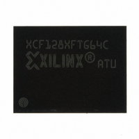
XCF128XFTG64C Xilinx Inc, XCF128XFTG64C Datasheet - Page 23

XCF128XFTG64C
Manufacturer Part Number
XCF128XFTG64C
Description
IC PROM SRL 128M GATE 64-FTBGA
Manufacturer
Xilinx Inc
Datasheet
1.XCF128XFTG64C.pdf
(88 pages)
Specifications of XCF128XFTG64C
Memory Size
128Mb
Programmable Type
In System Programmable
Voltage - Supply
1.7 V ~ 2 V
Operating Temperature
-40°C ~ 85°C
Package / Case
64-TBGA
Access Time
85ns
Supply Voltage Range
1.7V To 2V
Memory Case Style
FTBGA
No. Of Pins
64
Operating Temperature Range
-40°C To +85°C
Svhc
No SVHC (15-Dec-2010)
Package /
RoHS Compliant
Lead Free Status / RoHS Status
Lead free / RoHS Compliant
Other names
122-1578
Available stocks
Company
Part Number
Manufacturer
Quantity
Price
Company:
Part Number:
XCF128XFTG64C
Manufacturer:
XILINX
Quantity:
319
Part Number:
XCF128XFTG64C
Manufacturer:
XILINX/赛灵思
Quantity:
20 000
Block Protection Status Bit (SR1)
The Block Protection Status bit is used to identify if a
Program or Block Erase operation tried to modify the
contents of a locked or locked-down block. When this bit is
High (set to ‘1’), a program or erase operation was
attempted on a locked or locked-down block.
After set High, the Block Protection Status bit must be set
Low by a Clear Status Register command or a hardware
reset before a new program or erase command is issued;
otherwise, the new command appears to fail.
Bank Write/Multiple Word Program Status
Bit (SR0)
The Bank Write Status bit indicates whether the addressed
bank is busy performing a write or is ready to accept a new
write command (a program or erase command). In Buffer
Enhanced Factory Program mode, the Multiple Word
DS617 (v3.0.1) January 07, 2010
Product Specification
R
Platform Flash XL High-Density Configuration and Storage Device
www.xilinx.com
Program bit shows if the device is ready to accept a new
word to be programmed to the memory array.
The Bank Write Status bit should only be considered valid
when the Program/Erase Controller Status SR7 is Low
(set to ‘0’).
When both the Program/Erase Controller Status bit and the
Bank Write Status bit are Low (set to ‘0’), the addressed
bank is executing a program or erase operation. When the
Program/Erase Controller Status bit is Low (set to ‘0’) and
the Bank Write Status bit is High (set to ‘1’), a program or
erase operation is being executed in a bank other than the
one being addressed.
In Buffer Enhanced Factory Program mode, if Multiple Word
Program Status bit is Low (set to ‘0’), the device is ready for
the next word; if the Multiple Word Program Status bit is
High (set to ‘1’) the device is not ready for the next word.
For further details on how to use the Status Register, see
the Flowcharts and Pseudocodes provided in
Flowcharts and Pseudocodes," page
71.
"Appendix C:
23


