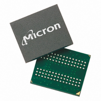
MT46H16M16LFBF-6 IT:A Micron Technology Inc, MT46H16M16LFBF-6 IT:A Datasheet - Page 23

MT46H16M16LFBF-6 IT:A
Manufacturer Part Number
MT46H16M16LFBF-6 IT:A
Description
IC DDR SDRAM 256MBIT 60VFBGA
Manufacturer
Micron Technology Inc
Type
DDR SDRAMr
Specifications of MT46H16M16LFBF-6 IT:A
Format - Memory
RAM
Memory Type
Mobile DDR SDRAM
Memory Size
256M (16Mx16)
Speed
166MHz
Interface
Parallel
Voltage - Supply
1.7 V ~ 1.95 V
Operating Temperature
-40°C ~ 85°C
Package / Case
60-VFBGA
Organization
16Mx16
Density
256Mb
Address Bus
15b
Access Time (max)
6.5/5ns
Maximum Clock Rate
166MHz
Operating Supply Voltage (typ)
1.8V
Package Type
VFBGA
Operating Temp Range
-40C to 85C
Operating Supply Voltage (max)
1.95V
Operating Supply Voltage (min)
1.7V
Supply Current
100mA
Pin Count
60
Mounting
Surface Mount
Operating Temperature Classification
Industrial
Lead Free Status / Rohs Status
Compliant
Other names
Q3368612
DESELECT
NO OPERATION (NOP)
LOAD MODE REGISTER
ACTIVE
READ
WRITE
PDF: 09005aef82091978 / Source: 09005aef8209195b
MT46H16M16LF__2.fm - Rev. H 6/08 EN
The DESELECT function (CS# HIGH) prevents new commands from being executed by
the Mobile DDR SDRAM. Operations already in progress are not affected.
The NO OPERATION (NOP) command is used to instruct the selected Mobile DDR
SDRAM to perform a NOP (CS# is LOW with RAS#, CAS#, and WE# HIGH). This prevents
unwanted commands from being registered during idle or wait states. Operations
already in progress are not affected.
The mode registers are loaded via inputs BA0–BA1 and A0–A12. See mode register
descriptions in “Register Definition” on page 15. The LOAD MODE REGISTER
command can only be issued when all banks are idle, and a subsequent executable
command cannot be issued until
The ACTIVE command is used to open (or activate) a row in a particular bank for a
subsequent access. The value on the BA0 and BA1 inputs selects the bank, and the
address provided on inputs A0–A12 selects the row. This row remains active (or open)
for accesses until a PRECHARGE command is issued to that bank. A PRECHARGE
command must be issued before opening a different row in the same bank.
The READ command is used to initiate a burst read access to an active row. The value on
the BA0, BA1 inputs selects the bank, and the address provided on inputs A0–Ai (where i
= the most significant column address bit for each configuration) selects the starting
column location. The value on input A10 determines whether auto precharge is used. If
auto precharge is selected, the row being accessed will be precharged at the end of the
READ burst; if auto precharge is not selected, the row will remain open for subsequent
accesses.
The WRITE command is used to initiate a burst write access to an active row. The value
on the BA0–BA1 inputs selects the bank, and the address provided on inputs A0–Ai
(where i = the most significant column address bit for each configuration) selects the
starting column location. The value on input A10 determines whether auto precharge is
used. If auto precharge is selected, the row being accessed will be precharged at the end
of the WRITE burst; if auto precharge is not selected, the row will remain open for subse-
quent accesses. Input data appearing on the DQ is written to the memory array subject
to the DM input logic level appearing coincident with the data. If a given DM signal is
registered LOW, the corresponding data will be written to memory; if the DM signal is
registered HIGH, the corresponding data inputs will be ignored, and a WRITE will not be
executed to that byte/column location.
23
t
MRD is met.
Micron Technology, Inc., reserves the right to change products or specifications without notice.
256Mb: x16, x32 Mobile DDR SDRAM
©2005 Micron Technology, Inc. All rights reserved.
Commands


