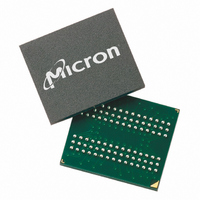
MT46H16M16LFBF-6 IT:A Micron Technology Inc, MT46H16M16LFBF-6 IT:A Datasheet - Page 16

MT46H16M16LFBF-6 IT:A
Manufacturer Part Number
MT46H16M16LFBF-6 IT:A
Description
IC DDR SDRAM 256MBIT 60VFBGA
Manufacturer
Micron Technology Inc
Type
DDR SDRAMr
Specifications of MT46H16M16LFBF-6 IT:A
Format - Memory
RAM
Memory Type
Mobile DDR SDRAM
Memory Size
256M (16Mx16)
Speed
166MHz
Interface
Parallel
Voltage - Supply
1.7 V ~ 1.95 V
Operating Temperature
-40°C ~ 85°C
Package / Case
60-VFBGA
Organization
16Mx16
Density
256Mb
Address Bus
15b
Access Time (max)
6.5/5ns
Maximum Clock Rate
166MHz
Operating Supply Voltage (typ)
1.8V
Package Type
VFBGA
Operating Temp Range
-40C to 85C
Operating Supply Voltage (max)
1.95V
Operating Supply Voltage (min)
1.7V
Supply Current
100mA
Pin Count
60
Mounting
Surface Mount
Operating Temperature Classification
Industrial
Lead Free Status / Rohs Status
Compliant
Other names
Q3368612
CAS Latency
Figure 6:
PDF: 09005aef82091978 / Source: 09005aef8209195b
MT46H16M16LF__2.fm - Rev. H 6/08 EN
Standard Mode Register Definition
The CAS latency is the delay, in clock cycles, between the registration of a READ
command and the availability of the first output data. The latency can be set to two or
three clocks, as shown in Figure 7 on page 18.
For CAS latency three (CL = 3), if the READ command is registered at clock edge n, then
the data will nominally be available at (n + 2 clocks +
command is registered at clock edge n, then the data will be nominally be available at (n
+ 1 clock +
M14
0
0
1
1
M13
0
1
0
1
14
0
BA1
M12 M11 M10 M9 M8 M7 M6–M0 Operating Mode
Mode Register Definition
Standard mode register
Reserved
Extended mode register
Reserved
0
–
BA0
0
13
t
AC).
12
A12 A11
0
–
Operating Mode
11
0
–
10
A10
0
–
9
A9
0
–
A8
8
7
A7 A6 A5 A4 A3
0
M6
–
CAS Latency BT
0
0
0
0
1
1
1
1
16
6
M5
Valid
0
0
1
1
0
0
1
1
5
M4
0
1
0
1
0
1
0
1
4
M3
All other states reserved
0
1
Normal operation
3
Micron Technology, Inc., reserves the right to change products or specifications without notice.
256Mb: x16, x32 Mobile DDR SDRAM
Burst Length
M2
CAS Latency
0
0
0
0
1
1
1
1
A2 A1 A0
2
Reserved
Reserved
Reserved
Reserved
Reserved
Reserved
M1
0
0
1
1
0
0
1
1
1
Interleaved
Burst Type
Sequential
2
3
M0
0
1
0
1
0
1
0
1
0
Reserved
Reserved
Reserved
Reserved
Reserved
M3 = 0
Standard Mode Register (Mx)
t
Address Bus
2
4
8
AC). For CL = 2, if the READ
Burst Length
Reserved
Reserved
Reserved
Reserved
Reserved
M3 = 1
©2005 Micron Technology, Inc. All rights reserved.
Register Definition
2
4
8


