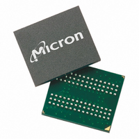
MT46H16M16LFBF-6 IT:A Micron Technology Inc, MT46H16M16LFBF-6 IT:A Datasheet - Page 22

MT46H16M16LFBF-6 IT:A
Manufacturer Part Number
MT46H16M16LFBF-6 IT:A
Description
IC DDR SDRAM 256MBIT 60VFBGA
Manufacturer
Micron Technology Inc
Type
DDR SDRAMr
Specifications of MT46H16M16LFBF-6 IT:A
Format - Memory
RAM
Memory Type
Mobile DDR SDRAM
Memory Size
256M (16Mx16)
Speed
166MHz
Interface
Parallel
Voltage - Supply
1.7 V ~ 1.95 V
Operating Temperature
-40°C ~ 85°C
Package / Case
60-VFBGA
Organization
16Mx16
Density
256Mb
Address Bus
15b
Access Time (max)
6.5/5ns
Maximum Clock Rate
166MHz
Operating Supply Voltage (typ)
1.8V
Package Type
VFBGA
Operating Temp Range
-40C to 85C
Operating Supply Voltage (max)
1.95V
Operating Supply Voltage (min)
1.7V
Supply Current
100mA
Pin Count
60
Mounting
Surface Mount
Operating Temperature Classification
Industrial
Lead Free Status / Rohs Status
Compliant
Other names
Q3368612
Commands
Table 7:
Table 8:
PDF: 09005aef82091978 / Source: 09005aef8209195b
MT46H16M16LF__2.fm - Rev. H 6/08 EN
Name (Function)
Name (Function)
DESELECT (NOP)
NO OPERATION (NOP)
ACTIVE (select bank and activate row)
READ (select bank and column, and start READ burst)
WRITE (select bank and column, and start WRITE burst)
BURST TERMINATE or deep power-down
(enter deep power-down mode)
PRECHARGE (deactivate row in bank or banks)
AUTO REFRESH (refresh all or single bank) or
SELF REFRESH (enter self refresh mode)
LOAD MODE REGISTER (standard or extended mode
registers)
Write enable
Write inhibit
Truth Table – Commands
Notes 1 and 2 apply to all commands
Truth Table – DM Operation
Notes:
Notes:
10. Internal refresh counter controls row addressing; all self refresh inputs and I/Os are “Don’t
11. BA0–BA1 either select the standard mode register or the extended mode register
Tables 7 and 8 provide a quick reference of available commands. This is followed by a
description of each command. Three additional truth tables provide CKE commands
and current/next state information (see Table 9 on page 51, Table 10 on page 52, and
Table 11 on page 54).
1. CKE is HIGH for all commands shown except SELF REFRESH and deep power-down.
2. All states and sequences not shown are reserved and/or illegal.
3. DESELECT and NOP are functionally interchangeable.
4. BA0–BA1 provide bank address and A0–A12/A13 provide row address.
5. BA0–BA1 provide bank address; A0–A8 provide column address; A10 HIGH enables the auto
6. Applies only to read bursts with auto precharge disabled; this command is undefined (and
7. This command is a BURST TERMINATE if CKE is HIGH and deep power-down if CKE is LOW.
8. A10 LOW: BA0–BA1 determine which bank is precharged.
9. This command is AUTO REFRESH if CKE is HIGH, SELF REFRESH if CKE is LOW.
1. Used to mask write data; provided coincident with the corresponding data.
2. All states and sequences not shown are reserved and illegal.
precharge feature (nonpersistent); A10 LOW disables the auto precharge feature.
should not be used) for READ bursts with auto precharge enabled and for WRITE bursts.
A10 HIGH: all banks are precharged and BA0
Care” except for CKE.
(BA0 = 0, BA1 = 0 select the standard mode register; BA0 = 0, BA1 = 1 select extended mode
register; other combinations of BA0–BA1 are reserved). A0–A12/A13 provide the op-code to
be written to the selected mode register.
22
CS#
H
L
L
L
L
L
L
L
L
DM
RAS#
H
L
X
H
H
H
H
Micron Technology, Inc., reserves the right to change products or specifications without notice.
L
L
L
L
256Mb: x16, x32 Mobile DDR SDRAM
–
CAS#
BA1 are “Don’t Care.”
X
H
H
H
H
L
L
L
L
WE#
H
H
H
H
X
L
L
L
L
Valid
DQ
X
©2005 Micron Technology, Inc. All rights reserved.
Bank/column
Bank/column
Bank/row
Address
Op-code
Code
X
X
X
X
Commands
Notes
1, 2
1, 2
Notes
9, 10
6, 7
11
3
3
4
5
5
8


