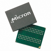
MT46H16M16LFBF-6 IT:A Micron Technology Inc, MT46H16M16LFBF-6 IT:A Datasheet - Page 20

MT46H16M16LFBF-6 IT:A
Manufacturer Part Number
MT46H16M16LFBF-6 IT:A
Description
IC DDR SDRAM 256MBIT 60VFBGA
Manufacturer
Micron Technology Inc
Type
DDR SDRAMr
Specifications of MT46H16M16LFBF-6 IT:A
Format - Memory
RAM
Memory Type
Mobile DDR SDRAM
Memory Size
256M (16Mx16)
Speed
166MHz
Interface
Parallel
Voltage - Supply
1.7 V ~ 1.95 V
Operating Temperature
-40°C ~ 85°C
Package / Case
60-VFBGA
Organization
16Mx16
Density
256Mb
Address Bus
15b
Access Time (max)
6.5/5ns
Maximum Clock Rate
166MHz
Operating Supply Voltage (typ)
1.8V
Package Type
VFBGA
Operating Temp Range
-40C to 85C
Operating Supply Voltage (max)
1.95V
Operating Supply Voltage (min)
1.7V
Supply Current
100mA
Pin Count
60
Mounting
Surface Mount
Operating Temperature Classification
Industrial
Lead Free Status / Rohs Status
Compliant
Other names
Q3368612
Figure 8:
Stopping the External Clock
PDF: 09005aef82091978 / Source: 09005aef8209195b
MT46H16M16LF__2.fm - Rev. H 6/08 EN
E14
E12
0
–
0
0
1
1
E11
E13
0
–
0
1
0
1
Extended Mode Register
E10
Mode Register Definition
Standard mode register
Reserved
Extended mode register
Reserved
0
–
Notes:
E9
0
–
14
1
BA1
E14
E8
0
–
1. On-die temperature sensor is used in place of TCSR. Setting these bits will have no effect.
One method of controlling the power efficiency in applications is to throttle the clock
that controls the DDR SDRAM. Control the clock in two ways:
• Change the clock frequency.
• Stop the clock.
The Mobile DDR SDRAM enables the clock to change frequency during operation only if
all the timing parameters are met and all refresh requirements are satisfied.
The clock can be stopped if no DRAM operations are in progress that would be affected
by this change. Any DRAM operation already in process must be completed before
entering clock stop mode; this includes the following timings:
t
For example, if a WRITE or a READ is in progress, the entire data burst must be complete
prior to stopping the clock. For READs, a burst completion is defined when the read
postamble is satisfied. For WRITEs, a burst completion is defined when the write post-
amble and
BA0 A12
E13
13
0
WR, and all data-out for READ bursts.
E7
0
–
12
E12
E6–E0
Valid
–
11
A11
E11
Set to “0”
t
WR or
10
A10
E10
Normal operation
All other states reserved
Operating Mode
A9
E9
9
E6
t
0
0
1
1
WTR are satisfied.
A8
E8
8
E5
0
1
0
1
A7
E7
7
A6
E6
6
DS
20
5
A5
E5
TCSR
4
A4
E4
E2
0
0
0
0
1
1
1
1
Micron Technology, Inc., reserves the right to change products or specifications without notice.
256Mb: x16, x32 Mobile DDR SDRAM
1
A3
3
E3
E1
0
0
1
1
0
0
1
1
A2
2
E0
E2
0
1
0
1
0
1
0
1
PASR
A1
1
E1
Partial-Array Self Refresh Coverage
Full array
Half array
Quarter array
Reserved
Reserved
One-eighth array
One-sixteenth array
Reserved
A0
0
E0
Address Bus
Extended Mode
Register
t
©2005 Micron Technology, Inc. All rights reserved.
RCD,
Register Definition
t
RP,
t
RFC,
t
MRD,


