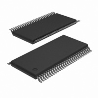
SC28L202A1DGG/G,11 NXP Semiconductors, SC28L202A1DGG/G,11 Datasheet - Page 55

SC28L202A1DGG/G,11
Manufacturer Part Number
SC28L202A1DGG/G,11
Description
IC UART DUAL W/FIFO 56-TSSOP
Manufacturer
NXP Semiconductors
Series
IMPACTr
Datasheet
1.SC28L202A1DGG118.pdf
(77 pages)
Specifications of SC28L202A1DGG/G,11
Features
False-start Bit Detection
Number Of Channels
2, DUART
Fifo's
256 Byte
Voltage - Supply
3.3V, 5V
With Parallel Port
Yes
With Auto Flow Control
Yes
With False Start Bit Detection
Yes
With Modem Control
Yes
With Cmos
Yes
Mounting Type
Surface Mount
Package / Case
56-TFSOP (0.240", 6.10mm Width)
Lead Free Status / RoHS Status
Lead free / RoHS Compliant
Other names
935279792118
SC28L202A1DGG/G-T
SC28L202A1DGG/G-T
SC28L202A1DGG/G-T
SC28L202A1DGG/G-T
Philips Semiconductors
OPCR Output Port Configuration Register. Controls [7:2] B
NOTE: I/O0 B and I/O1 B output OPR(0) and OPR(1) respectively.
Under program control of MR1 and MR2 the signals RTSN A for
I/O0 B and RTSN B for I/O1 B may be assigned.
OPCR[7] – This bit programs the I/O7 B output to provide one of the
following:
OPCR[6] – This bit programs the I/O6 B output to provide one of the
following:
OPCR[5] – This bit programs the I/O5 B output to provide one of the
following:
OPCR[4] – This field programs the I/O4 B output to provide one of
the following:
2005 Nov 01
0 The complement of OPR[7].
1 The Channel B transmitter interrupt output which is the
complement of ISR[4]. When in this mode I/O7 acts as an open–
drain output. Note that this output is not masked by the contents
of the IMR.
0 The complement of OPR[6].
1 The Channel A transmitter interrupt output which is the
complement of ISR[0]. When in this mode I/O6 acts as an open–
drain output. Note that this output is not masked by the contents
of the IMR.
0 The complement of OPR[5].
1 The Channel B receiver interrupt output which is the
complement of ISR[5]. When in this mode I/O5 acts as an
open–drain output. Note that this output is not masked by the
contents of the IMR.
0 The complement of OPR[4].
1 The Channel A receiver interrupt output which is the
complement of ISR[1]. When in this mode I/O4 acts as an
Dual UART
Bit 7
I/O7 B
0 = OPR[7]
1 = Tx RDY B
BIT 6
I/O6 B
0 = OPR[6]
1 = Tx RDY A
BIT 5
I/O5 B
0 = OPR[5]
1 = Rx RDY / FFULL B
49
BIT 4
I/O4 B
0 = OPR[4]
1 = Rx RDY / FFULL A
OPCR[3:2] – This bit programs the I/O3 B output to provide one of
the following:
OPCR[1:0] – This field programs the I/O2 B output to provide one of
the following:
open–drain output. Note that this output is not masked by the
contents of the IMR.
00 The complement of OPR[3].
01 The counter/timer output, in which case I/O3 acts as an
open–drain output. In the timer mode, this output is a square wave
at the programmed frequency. In the counter mode, the output
remains high until terminal count is reached, at which time it goes
low. The output returns to the high state when the counter is
stopped by a stop counter command. Note that this output is not
masked by the contents of the IMR.
10 The 1X clock for the Channel B transmitter that shifts the
transmitted data. If data is not being transmitted, a free running 1X
clock is output.
11 The 1X clock for the Channel B receiver that samples the
received data. If data is not being received, a free running 1X
clock is output.
00 The complement of OPR[2].
01 The 16X clock for the Channel A transmitter. This is the clock
selected by CSR A [3:0], and will be a 1X clock if CSR A [3:0] =
1111.
10 The 1X clock for the Channel A transmitter that shifts the
transmitted data. If data is not being transmitted, a free running 1X
clock is output.
11 The 1X clock for the Channel A receiver that samples the
received data. If data is not being received, a free running 1X
clock is output.
BIT (3:2)
I/O3 B
00 = OPR[3]
01 = C/T OUTPUT
10 = TxC B(1X)
11 = RxC B(1X)
SC28L202
BIT (1:0)
I/O2 B
00 = OPR[2]
01 = TxC A(16X)
10 = TxC A(1X)
11 = RxC A(1X)
Product data sheet


