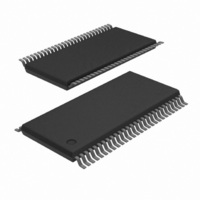
SC28L202A1DGG/G,11 NXP Semiconductors, SC28L202A1DGG/G,11 Datasheet - Page 30

SC28L202A1DGG/G,11
Manufacturer Part Number
SC28L202A1DGG/G,11
Description
IC UART DUAL W/FIFO 56-TSSOP
Manufacturer
NXP Semiconductors
Series
IMPACTr
Datasheet
1.SC28L202A1DGG118.pdf
(77 pages)
Specifications of SC28L202A1DGG/G,11
Features
False-start Bit Detection
Number Of Channels
2, DUART
Fifo's
256 Byte
Voltage - Supply
3.3V, 5V
With Parallel Port
Yes
With Auto Flow Control
Yes
With False Start Bit Detection
Yes
With Modem Control
Yes
With Cmos
Yes
Mounting Type
Surface Mount
Package / Case
56-TFSOP (0.240", 6.10mm Width)
Lead Free Status / RoHS Status
Lead free / RoHS Compliant
Other names
935279792118
SC28L202A1DGG/G-T
SC28L202A1DGG/G-T
SC28L202A1DGG/G-T
SC28L202A1DGG/G-T
Philips Semiconductors
RxCSR – Receiver Clock Select Register A and B
TxCSR Transmitter Clock Select Register A and B
Both registers consist of single 6-bit field that selects the clock source for the receiver and transmitter respectively. During a read the unused
bits in this register read b’000. The ‘BRG’ baud rates (fixed BRG rates) shown in the table below are based on the Sclk crystal frequency of
14.7456 MHz. The baud rates shown below will vary as the Sclk crystal clock varies. For example, if the Sclk rate is changed to 7.3728 MHz all
the rates below will reduce by 1/2.
Rx and Tx Clock Select Table
NOTE: Sclk maximum rate is 50 MHz. Data clock rates will follow exactly the ratio of the X1/Sclk to 14.7654 MHz
This field selects the baud rate clock for the Channel A transmitter.
* External clock Pin and external clock mode assignment.
2005 Nov 01
Tx A Clock Select Code
00 0000
00 0001
00 0010
00 0011
00 0100
00 0101
00 0110
00 0111
00 1000
00 1001
00 1010
00 1011
00 1100
00 1101
00 1110
00 1111
Tx A Clock Select Code
Tx/Rx CSR x [5:0]
001110
001111
Dual UART
Bit 7
Reserved
Clock selection, Sclk = 14.7456 MHz
BRG – 50
BRG – 110
BRG – 134.5
BRG – 200
BRG – 300
BRG – 600
BRG – 1200
BRG – 1050
BRG – 2400
BRG – 4800
BRG – 7200
BRG – 9600
BRG – 38.4K
Timer 0
I/O3 A transmitter – 16x External *
I/O3 A transmitter – 1x External *
Clock selection, Sclk = 14.7456 MHz
RxC Channel A
I/O4 A 16x
I/O4 A 1X
Bit 6
Reserved
Bits 5:0
Transmitter/Receiver Clock select code,
See Clock Multiplex Table below
24
Tx A Clock Select Code
01 0000
01 0001
01 0010
01 0011
01 0100
01 0101
01 0110
01 0111
01 1000
01 1001
01 1010
01 1011
01 1100
01 1101
01 1110
01 1111
Tx A Clock Select Code
11 0000 to 11 1101
11 1110
11 1111
TxC Channel B
I/O5 A 16x
I/O5 A 1X
Clock selection, Sclk = 14.7456 MHz
BRG – 75
BRG – 150
BRG – 450
BRG – 1800
BRG – 2000
BRG – 14.4K
BRG – 19.2K
BRG – 28.8K
BRG – 57.6K
BRG – 115.2K
BRG – 230.4K
BRG – 460.8K
BRG – 921.6K
Timer 1
PBRG 0
Midi rate 31.25 KHz 1.66% error
Clock selection, Sclk = 14.7456 MHz
Reserved
PBRG 1
Reserved
RxC channel B
I/O6 A 16x
I/O6 A 1X
SC28L202
Product data sheet


