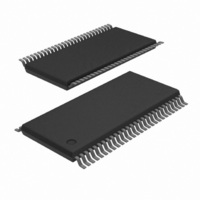
SC28L202A1DGG/G,11 NXP Semiconductors, SC28L202A1DGG/G,11 Datasheet - Page 24

SC28L202A1DGG/G,11
Manufacturer Part Number
SC28L202A1DGG/G,11
Description
IC UART DUAL W/FIFO 56-TSSOP
Manufacturer
NXP Semiconductors
Series
IMPACTr
Datasheet
1.SC28L202A1DGG118.pdf
(77 pages)
Specifications of SC28L202A1DGG/G,11
Features
False-start Bit Detection
Number Of Channels
2, DUART
Fifo's
256 Byte
Voltage - Supply
3.3V, 5V
With Parallel Port
Yes
With Auto Flow Control
Yes
With False Start Bit Detection
Yes
With Modem Control
Yes
With Cmos
Yes
Mounting Type
Surface Mount
Package / Case
56-TFSOP (0.240", 6.10mm Width)
Lead Free Status / RoHS Status
Lead free / RoHS Compliant
Other names
935279792118
SC28L202A1DGG/G-T
SC28L202A1DGG/G-T
SC28L202A1DGG/G-T
SC28L202A1DGG/G-T
Philips Semiconductors
REGISTER DESCRIPTION AND PROGRAMMING
NOTE
Programmers may use either of two register sets or mix the features
of each. It is suggested that only the extended register set be used
in new designs. However if a system needed to use a block of
communications code written for an older system then that code
could merely be called. This is similar to calling a DOS program in
a WINDOWS environment. Before calling legacy code it is
recommended (but not required) to execute ‘Reset to C92’
command. Also consideration must be given to the I/O pins to avoid
contention of drivers of the pins and an external driver.
Two control register descriptions and maps are implemented in the
SC28L92: one represents the previous 4-bit address and the other
the new 7-bit address space representing the all the new features of
the new design.
The Design of the SC28L202 allows for high degree with former
Philips two channel communications controllers—DUARTs.
Table 2. SC28L202 REGISTER BIT DESCRIPTIONS
Registers that control Global Properties of the 28L202
GCCR – Global Configuration Control Register
THIS IS A VERY IMPORTANT REGISTER! IT SHOULD BE THE FIRST REGISTER ADDRESSED DURING INITIALIZATION.
GCCR(7:6) DACKN Assertion
Motorola bus cycle time can be controlled by selecting a DACKN
assertion time based on X1/Sclk speed. The time programmed
should not be less than the minimum read or write pulse width.
See examples below.
GCCR(5:3): Reserved
GCCR(2:1): Interrupt vector configuration
The IVC field controls if and how the assertion of IACKN (the
interrupt acknowledge pin) will form the interrupt vector for the
DUART. If b’00, no vector will be presented during an IACKN cycle.
The bus will be driven high (0xFF). If the field contains a b’01, the
contents of the IVR, Interrupt Vector Register, will be presented as
the interrupt vector without modification.
2005 Nov 01
Hex
Addr
X1/SCLK
3.6864 MHz
7.3728 MHz
14.7456 MHz
29.4912 MHz
33.1776 MHz
44.2368 MHz
Dual UART
Bit [7:6]
DACKN Assertion
00 = 2 – 3 Sclk
01 = 1 – 2 Sclk
10 = 1/2 – 1 Sclk
11 = Reserved
#SCLK Cycles
1/2–1
1/2–1
1/2–1
1–2
2–3
2–3
Bit [5:3]
Reserved
Set to 0
Delay
136–272 ns
68–136 ns
34–68 ns
34–68 ns
60–90 ns
46–68 ns
Bit [2:1]
IVC Interrupt Vector Control
00 = no interrupt vector
01 = IVR[7:0]
10 = IVR[7:1] + channel code
11 = IVR[7:5] + interrupt type + channel code
18
To facilitate this feature the complete register function and control of
the SC26C92 is replicated in the SC28L202. That is code written for
the SCN2681, SCN68681, SCC2692, SCC68692 and SC26C92 will
operate with this device.
With the execution of code written for previous DUARTs and
immediately after a hardware reset or a ‘Reset to C92’ command the
following configuration will exist:
1. The size of all FIFOs is set to 8 bytes (for legacy code).
2. FIFO interrupt levels are controlled by the bits of the MR
3. All I/O ports are set to input.
4. Receiver FIFO set to interrupt on FIFO ready.
5. Transmitter FIFO set to interrupt on FIFO empty.
6. Baud selection follows previous 4 bit programming and baud rate
If IVC = 0x10, the channel code will replace the LSB of the IVR; if
IVC = b’11 then a modified interrupt type and channel code replace
the 3 LSBs of the IVR. NOTE: The modified type field IVR[2:1] is:
GCCR(0): Interrupt Status Masking
This bit controls the readout mode of the Interrupt Status Register,
ISR. If set, the ISR reads the current status masked by the IMR, i.e.
only interrupt sources enabled in the IMR can ever show a ‘1’ in the
ISR. If cleared, the ISR shows the current status of the interrupt
source without regard to the Interrupt Mask setting.
10 Receiver w/o error
11 Receiver with error
01 Transmitter
00 All remaining sources
registers
grouping controlled by the MR and ACR registers.
BIT 0
ISR Read Mode
0 = ISR Unmasked
1 = ISR Read Masked by IMR
SC28L202
Product data sheet


