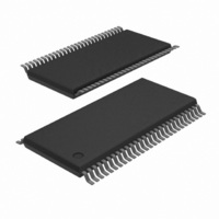
SC28L202A1DGG/G,11 NXP Semiconductors, SC28L202A1DGG/G,11 Datasheet - Page 43

SC28L202A1DGG/G,11
Manufacturer Part Number
SC28L202A1DGG/G,11
Description
IC UART DUAL W/FIFO 56-TSSOP
Manufacturer
NXP Semiconductors
Series
IMPACTr
Datasheet
1.SC28L202A1DGG118.pdf
(77 pages)
Specifications of SC28L202A1DGG/G,11
Features
False-start Bit Detection
Number Of Channels
2, DUART
Fifo's
256 Byte
Voltage - Supply
3.3V, 5V
With Parallel Port
Yes
With Auto Flow Control
Yes
With False Start Bit Detection
Yes
With Modem Control
Yes
With Cmos
Yes
Mounting Type
Surface Mount
Package / Case
56-TFSOP (0.240", 6.10mm Width)
Lead Free Status / RoHS Status
Lead free / RoHS Compliant
Other names
935279792118
SC28L202A1DGG/G-T
SC28L202A1DGG/G-T
SC28L202A1DGG/G-T
SC28L202A1DGG/G-T
Philips Semiconductors
IPCE – Input Change Detect Enable, A and B (n = A for A, n = B for B)
IPCE[7:0] bits activate the input change of state detectors. If a pin is configured as an output, the change of state detectors, if enabled, continue
to be active and will show a change of state as the I/P port changes.
I/OPCR 0 – I/O Port Configuration Register
I/OPCR 1 – I/O Port Configuration Register
I/OPCR 2 – I/O Port Configuration Register
I/OPCR 3 – I/O Port Configuration Register
NOTE: Both I/O Port A and B default to input upon a hardware reset to avoid hardware conflicts with I/O direction
The four registers above contain 4, 2 bit fields that set the direction and source for each of the I/O pins associated with the channel. The I/O0 B
or I/O1 B output may be RTSN if MR1[7] is set. It may also signal ‘end of transmission’ if MR2[5] is set. (Please see the descriptions of these
functions under the MR1 and MR2 register descriptions).
The binary settings of the binary 00 combination always configures the I/O pins as ‘inputs’. However the input circuit of the I/O pins are ALWAYS
active. In actuality the binary 00 condition only disable the output driver of the pin. Since the input circuit and the associated change of state
detector is always active the output signal may generate interrupts or drive counters.
This register resets to 0x00 on reset, effectively configuring all I/O pins as inputs. Inputs may be used as RxC, TxC inputs or CTSN and General
Purpose Inputs simultaneously. All inputs are equipped with change detectors that may be used to generate interrupts or can be polled, as
required.
2005 Nov 01
Bit 7
0 = disable
1 = enable
Bits 7:6
I/O3 A control
00 = GPI / TxC A
01 = OPR[3] A
10 = TxC A (16X) Output
11 = Reserved
Bits 7:6
I/O7 A control
00 = GPI / CT 1 Clock Input
01 = OPR[7] A / DTRN B
10 = TxC B (1X) Output
11 = Reserved
Bits 7:6
I/O3 B control
00 = GPI /DSRN B
01 = OPR[3] B
10 = RxC B (1X) Output
11 = C/T 0 Output (open
drain)
Bits 7:6
I/O7 B control
00 = GPI /RIN B
01 = OPR[7] B
10 =TxINTN B (open drain)
11 =reserved
I/O7 n enable
Dual UART
Bit 6
0 = disable
1 = enable
I/O6 n enable
Bits 5:4
I/O2 A control
00 = GPI / CT 0 Clock Input
01 = OPR[2] A / DTRN A
10 = TxC A (1X) Output
11 = Reserved
Bits 5:4
I/O6 B control
00 = GPI /RIN A
01 = OPR[6] B
10 =TxINTN A (open drain)
11 = reserved
Bits 5:4
I/O2 B control
00 = GPI /DSRN A
01 = OPR[2] B
10 = RxC A (1X) Output
11 = C/T 1 Output (open drain)
Bits 5:4
I/O6 A control
00 = GPI / RxC B / PBRG 1 Clk Input
01 = OPR[6] A
10 = RxC B (16X) Output
11 = Reserved
Bit 5
0 = disable
1 = enable
I/O5 n enable
Bit 4
0 = disable
1 = enable
I/O4 n enable
37
Bit 3
0 = disable
1 = enable
I/O3 n enable
Bits 3:2
I/O1 B control
00 = GPI
01 = OPR[1] B / RTSN B
10 = Reserved
11 = Reserved
Bits 3:2
I/O5 B control
00 = GPI /DCDN B
01 = OPR[5] B
10 = RxINTN B (open
drain)
11 = reserved
Bits 3:2
I/O5 A control
00 = GPI / TxC B
01 = OPR[5] A
10 = TxC B (16X) Output
11 = Reserved
Bits 3:2
I/O1 A control
00 = GPI / CTSN B
01 = OPR[1] A
10 –
11 = Reserved
Bit 2
0 = disable
1 = enable
I/O2 n enable
Bits 1:0
I/O4 B control
00 = GPI /DCDN A
01 = OPR[4] B
10 = RxINTN A (open drain)
11 = reversed
Bits 1:0
I/O0 B control
00 = GPI
01 = OPR[0] B / RTSN B
10 = Reserved
11 = Reserved
Bits 1:0
I/O0 A control
00 = GPI / CTSN A
01 = OPR[0] A
10 –
11 = Reserved
Bits 1:0
I/O4 A control
00 = GPI / RxC A / PBRG 0 Clk Input
01 = OPR[4] A
10 = RxC A (16X) Output
11 = Reserved
Bit 1
0 = disable
1 = enable
I/O1 n enable
SC28L202
Product data sheet
Bit 0
0 = disable
1 = enable
I/O0 n enable


