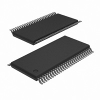
SC28L202A1DGG/G,11 NXP Semiconductors, SC28L202A1DGG/G,11 Datasheet - Page 38

SC28L202A1DGG/G,11
Manufacturer Part Number
SC28L202A1DGG/G,11
Description
IC UART DUAL W/FIFO 56-TSSOP
Manufacturer
NXP Semiconductors
Series
IMPACTr
Datasheet
1.SC28L202A1DGG118.pdf
(77 pages)
Specifications of SC28L202A1DGG/G,11
Features
False-start Bit Detection
Number Of Channels
2, DUART
Fifo's
256 Byte
Voltage - Supply
3.3V, 5V
With Parallel Port
Yes
With Auto Flow Control
Yes
With False Start Bit Detection
Yes
With Modem Control
Yes
With Cmos
Yes
Mounting Type
Surface Mount
Package / Case
56-TFSOP (0.240", 6.10mm Width)
Lead Free Status / RoHS Status
Lead free / RoHS Compliant
Other names
935279792118
SC28L202A1DGG/G-T
SC28L202A1DGG/G-T
SC28L202A1DGG/G-T
SC28L202A1DGG/G-T
Philips Semiconductors
Programmable Counters, Timers and Baud Rate generators
PBRGPU – Programmable BRG Timer Reload Registers, Upper 0 and 1
This is the upper byte of the 16–bit value used by the BRG timer in generating a baud rate clock
PBRGPL – Programmable BRG Timer Reload Registers, Lower 0 and 1
This is the lower byte of the 16–bit value used by the BRG timer in generating a baud rate clock.
CTCS 0 and 1 – Counter Timer clock source
NOTE: Writing to this register removes the control established in the counter/timer portion of the ACR in the default register map
CTVU – Counter Timer Value Registers, Upper 0 and 1
Reading this register gives the value of the upper 8 bits of the counter timer.
CTVL – Counter timer Value Registers, Lower 0 and 1
Reading this register gives the value of the upper 8 bits of the
counter timer.
NOTE: The counter timer should be stopped before reading. Usually
the clock of the counter timer is not synchronized with the read of
the C/T. It is therefore possible to capture changing data during the
read. Depending on the clock speed with respect to the read cycle
PBRGCS – Programmable BRG Clock Source
Start/Stop control and clock select register for the two BRG
counters. The clock selection is for the input to the counters. It is
that clock divided by the number represented by the PBRGPU and
PBRGPL the will be used as the 16x clock for the receivers and
transmitters. When the BRG timer Clock is selected for the
2005 Nov 01
Dual UART
Bits 7:0
8 MSBs of the BRG Timer divisor.
Bits 7:0
8 LSB of the BRG Timer divisor.
Bits 7:0
8 MSBs of the Counter timer preset value
Bits 7:0
8 LSB of the Counter timer preset value
Bit 7
PBRG 1, Register control
0 = Resets PBRG 1 and
holds it stopped
1 = Allows PBRG 1 to run.
Bit 7:6
Reserved
Bit 5:4
Mode control
00 – Selects Counter Mode. Generates
01 – Selects Timer Mode. Generates a
10 – Reserved
11 – Selects Timer Pulse Mode.
a timing edge
square wave
Generates periodic pulses twice the
the C/T. (i.e. after any prescale)
frequency as in Timer Mode. Pulse width
is one cycle of the clock as it is delivered to
Bit 6:4
PBRG 1, Clock selection
000 = Sclk
001 = Sclk / 2
010 = Sclk/ 16
011 = Sclk / 32
100 = Sclk / 64
101 = Sclk / 128
110 = I/O4 A
111 = Reserved
32
this could be made worse or completely eliminated. If the Stop
counter command is issued and following that the C/T is read there
will be no uncertainty go its value. If it is necessary to read the C/T
‘on the fly’ then reading it twice and comparing the values will
correct the problem. The double read will not be effective if the
counter timer clock is faster than a read cycle.
receiver(s) or transmitter(s) the receivers and transmitters will
consider it as a 16x clock and further device it by 16. In other words
the receivers and transmitters will always be in the 16x ode of
operation when the internal BRG timer is selected for their clock.
Bit 3
PBRG 0, Register control
0 = Resets PBRG 0 and
holds it stopped.
1 = Allows PBRG 0 to run.
Bit 3:0
Clock selection
0000 External I/O2 A (for CT 0), I/O7 A (for CT 1)
0001 External I/O2 A/16 (for CT 0), I/O7 A/16 (for CT 1)
0010 Sclk
0011 Sclk / 2
0100 Sclk / 16
0101 Sclk / 32
0110 Sclk / 64
0111 Sclk / 128
TxC1X A
TxC1X B
1010, 1011 Reserved
1100 Rx Character Count (Ch A) Clock is RxFIFO A load pulse
1101 Rx Character Count (Ch B) Clock is RxFIFO B load pulse
1110, 1111 Reserved
Bit 2:0
PBRG 0, Clock selection
000 = Sclk
001 = Sclk / 2
010 = Sclk / 16
011 = Sclk / 32
100 = Sclk / 64
101 = Sclk / 128
110 = I/O3 A
111 = Reserved
SC28L202
Product data sheet


