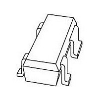
BF1202WR NXP Semiconductors, BF1202WR Datasheet - Page 4

BF1202WR
Manufacturer Part Number
BF1202WR
Description
Enhancement type Field-Effect Transistor in a plastic SOT343R package
Manufacturer
NXP Semiconductors
Datasheet
1.BF1202WR.pdf
(15 pages)
Specifications of BF1202WR
Application
VHF/UHF
Channel Type
N
Channel Mode
Enhancement
Continuous Drain Current
0.03A
Drain Source Voltage (max)
10V
Power Gain (typ)@vds
34.5@5VdB
Noise Figure (max)
11dB
Package Type
CMPAK
Pin Count
3 +Tab
Input Capacitance (typ)@vds
1.7@5V@Gate 1/1@5V@Gate 2pF
Output Capacitance (typ)@vds
0.85@5VpF
Reverse Capacitance (typ)
0.015@5VpF
Operating Temp Range
-65C to 150C
Mounting
Surface Mount
Number Of Elements
1
Power Dissipation (max)
200mW
Screening Level
Military
Lead Free Status / Rohs Status
Compliant
Available stocks
Company
Part Number
Manufacturer
Quantity
Price
Company:
Part Number:
BF1202WR
Manufacturer:
NXP
Quantity:
120 000
Company:
Part Number:
BF1202WR
Manufacturer:
PHILIPS
Quantity:
12 458
Part Number:
BF1202WR
Manufacturer:
NXP/恩智浦
Quantity:
20 000
NXP Semiconductors
STATIC CHARACTERISTICS
T
Note
1. R
DYNAMIC CHARACTERISTICS
Common source; T
Note
1. Measured in Fig.21 test circuit.
2010 Sep 16
V
V
V
V
V
V
V
I
I
I
y
C
C
C
C
F
G
X
SYMBOL
SYMBOL
j
DSX
G1-SS
G2-SS
= 25 C unless otherwise specified.
(BR)DSS
(BR)G1-SS
(BR)G2-SS
(F)S-G1
(F)S-G2
G1-S(th)
G2-S(th)
mod
N-channel dual-gate PoLo MOS-FETs
ig1-ss
ig2-ss
oss
rss
tr
fs
G1
connects G
drain-source breakdown voltage
gate 1-source breakdown voltage
gate 2-source breakdown voltage
forward source-gate 1 voltage
forward source-gate 2 voltage
gate 1-source threshold voltage
gate 2-source threshold voltage
drain-source current
gate 1 cut-off current
gate 2 cut-off current
forward transfer admittance
input capacitance at gate 1
input capacitance at gate 2
output capacitance
reverse transfer capacitance f = 1 MHz
noise figure
power gain
cross-modulation
amb
1
PARAMETER
to V
= 25 C; V
PARAMETER
GG
= 5 V.
G2-S
= 4 V; V
pulsed; T
f = 1 MHz
f = 1 MHz
f = 1 MHz
f = 10.7 MHz; G
f = 400 MHz; Y
f = 800 MHz; Y
f = 200 MHz; G
G
f = 400 MHz; G
G
f = 800 MHz; G
G
input level for k = 1%; f
f
unw
L
L
L
at 0 dB AGC
at 10 dB AGC
at 40 dB AGC
DS
= 0.5 mS; B
= 1 mS; B
= 1 mS; B
= 60 MHz; note 1
= 5 V; I
V
V
V
V
V
V
V
V
note 1
V
V
j
G1-S
G2-S
G1-S
G2-S
G1-S
G2-S
G1-S
G2-S
G2-S
G1-S
= 25 C
D
CONDITIONS
L
L
= V
= V
= V
= V
= V
= 4 V; V
= 5 V; V
= 4 V; V
= V
= V
= B
= B
= 12 mA; unless otherwise specified.
S
S
S
L
S
S
4
S
= Y
= Y
= B
= 2 mS; B
= 2 mS; B
= 3.3 mS; B
= 20 mS; B
G2-S
DS
DS
DS
DS
DS
DS
L opt
L opt
S opt
S opt
L opt
= 0; I
= 0; I
= 0; I
= 0; I
= 0; V
= 0; V
CONDITIONS
= 0; I
DS
DS
DS
w
= 50 MHz;
= 5 V; I
= 5 V; I
= 5 V; R
BF1202; BF1202R; BF1202WR
G1-S
G2-S
S-G1
S-G2
G1-S
G2-S
S
S
D
= B
= B
S
S
= 10 A
= 10 mA
= 10 mA
= 10 mA
= 10 mA
= 0
= B
= 5 V
= 4 V
S opt
S opt
D
D
G1
S opt
= 100 A
= 100 A
;
;
= 120 k;
;
25
90
100
MIN.
10
6
6
0.5
0.5
0.3
0.3
8
30
1.7
1
0.85
15
9
0.9
1.1
34.5
30.5
26.5
92
105
TYP.
MIN.
Product specification
1.5
1.5
1.0
1.2
16
50
20
40
2.2
30
11
1.5
1.8
MAX.
MAX.
V
V
V
V
V
V
V
mA
nA
nA
mS
pF
pF
pF
fF
dB
dB
dB
dB
dB
dB
dBV
dBV
dBV
UNIT
UNIT


