BF1202WR NXP Semiconductors, BF1202WR Datasheet - Page 2
BF1202WR
Manufacturer Part Number
BF1202WR
Description
Enhancement type Field-Effect Transistor in a plastic SOT343R package
Manufacturer
NXP Semiconductors
Datasheet
1.BF1202WR.pdf
(15 pages)
Specifications of BF1202WR
Application
VHF/UHF
Channel Type
N
Channel Mode
Enhancement
Continuous Drain Current
0.03A
Drain Source Voltage (max)
10V
Power Gain (typ)@vds
34.5@5VdB
Noise Figure (max)
11dB
Package Type
CMPAK
Pin Count
3 +Tab
Input Capacitance (typ)@vds
1.7@5V@Gate 1/1@5V@Gate 2pF
Output Capacitance (typ)@vds
0.85@5VpF
Reverse Capacitance (typ)
0.015@5VpF
Operating Temp Range
-65C to 150C
Mounting
Surface Mount
Number Of Elements
1
Power Dissipation (max)
200mW
Screening Level
Military
Lead Free Status / Rohs Status
Compliant
Available stocks
Company
Part Number
Manufacturer
Quantity
Price
Company:

Part Number:
BF1202WR
Manufacturer:
NXP
Quantity:
120 000
Company:
Part Number:
BF1202WR
Manufacturer:
PHILIPS
Quantity:
12 458
Part Number:
BF1202WR
Manufacturer:
NXP/恩智浦
Quantity:
20 000


NXP Semiconductors
FEATURES
Short channel transistor with high
Low noise gain controlled amplifier
Partly internal self-biasing circuit to
APPLICATIONS
VHF and UHF applications with
DESCRIPTION
Enhancement type N-channel
field-effect transistor with source and
substrate interconnected. Integrated
diodes between gates and source
protect against excessive input
voltage surges. The BF1202,
BF1202R and BF1202WR are
encapsulated in the SOT143B,
SOT143R and SOT343R plastic
packages respectively.
QUICK REFERENCE DATA
2010 Sep 16
V
I
P
y
C
C
F
X
T
SYMBOL
This product is supplied in anti-static packing to prevent damage caused by electrostatic discharge during transport
and handling.
D
forward transfer admittance to input
capacitance ratio
ensure good cross-modulation
performance during AGC and good
DC stabilization.
3 to 9 V supply voltage, such as
digital and analogue television
tuners and professional
communications equipment.
j
DS
tot
mod
N-channel dual-gate PoLo MOS-FETs
ig1-ss
rss
fs
drain-source voltage
drain current
total power dissipation
forward transfer admittance
input capacitance at gate 1
reverse transfer capacitance
noise figure
cross-modulation
operating junction temperature
PARAMETER
PINNING
Marking code legend:
handbook, 2 columns
* = - : made in Hong Kong
* = p : made in Hong Kong
* = t : made in Malaysia
BF1202 marking code: LD*
Fig.1
PIN
1
2
3
4
f = 800 MHz
input level for k = 1% at
f = 1 MHz
40 dB AGC
Top view
4
1
Simplified outline
(SOT143B).
CAUTION
CONDITIONS
2
source
drain
gate 2
gate 1
DESCRIPTION
MSB014
3
2
BF1202; BF1202R; BF1202WR
25
100
lfpage
MIN.
handbook, 2 columns
BF1202R marking code: LE*
Fig.2
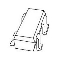
BF1202WR marking code: LE*
Fig.3
30
1.7
15
1.1
105
TYP.
3
2
Top view
3
2
Top view
Simplified outline
(SOT143R).
Simplified outline
(SOT343R).
Product specification
10
30
200
40
2.2
30
1.8
150
MAX.
MSB842
4
1
MSB035
4
1
V
mA
mW
mS
pF
fF
dB
dBV
C
UNIT
Related parts for BF1202WR
Image
Part Number
Description
Manufacturer
Datasheet
Request
R

Part Number:
Description:
Enhancement type Field-Effect Transistor in a plastic SOT143B package
Manufacturer:
NXP Semiconductors
Datasheet:

Part Number:
Description:
MOSFET 2N-CH 10V 30MA SOT143R
Manufacturer:
NXP Semiconductors
Datasheet:

Part Number:
Description:
NXP Semiconductors designed the LPC2420/2460 microcontroller around a 16-bit/32-bitARM7TDMI-S CPU core with real-time debug interfaces that include both JTAG andembedded trace
Manufacturer:
NXP Semiconductors
Datasheet:

Part Number:
Description:
NXP Semiconductors designed the LPC2458 microcontroller around a 16-bit/32-bitARM7TDMI-S CPU core with real-time debug interfaces that include both JTAG andembedded trace
Manufacturer:
NXP Semiconductors
Datasheet:
Part Number:
Description:
NXP Semiconductors designed the LPC2468 microcontroller around a 16-bit/32-bitARM7TDMI-S CPU core with real-time debug interfaces that include both JTAG andembedded trace
Manufacturer:
NXP Semiconductors
Datasheet:
Part Number:
Description:
NXP Semiconductors designed the LPC2470 microcontroller, powered by theARM7TDMI-S core, to be a highly integrated microcontroller for a wide range ofapplications that require advanced communications and high quality graphic displays
Manufacturer:
NXP Semiconductors
Datasheet:
Part Number:
Description:
NXP Semiconductors designed the LPC2478 microcontroller, powered by theARM7TDMI-S core, to be a highly integrated microcontroller for a wide range ofapplications that require advanced communications and high quality graphic displays
Manufacturer:
NXP Semiconductors
Datasheet:
Part Number:
Description:
The Philips Semiconductors XA (eXtended Architecture) family of 16-bit single-chip microcontrollers is powerful enough to easily handle the requirements of high performance embedded applications, yet inexpensive enough to compete in the market for hi
Manufacturer:
NXP Semiconductors
Datasheet:
Part Number:
Description:
The XA-S3 device is a member of Philips Semiconductors? XA(eXtended Architecture) family of high performance 16-bitsingle-chip microcontrollers
Manufacturer:
NXP Semiconductors
Datasheet:

Part Number:
Description:
The NXP BlueStreak LH75401/LH75411 family consists of two low-cost 16/32-bit System-on-Chip (SoC) devices
Manufacturer:
NXP Semiconductors
Datasheet:
Part Number:
Description:
The NXP LPC3130/3131 combine an 180 MHz ARM926EJ-S CPU core, high-speed USB2
Manufacturer:
NXP Semiconductors
Datasheet:
Part Number:
Description:
The NXP LPC3141 combine a 270 MHz ARM926EJ-S CPU core, High-speed USB 2
Manufacturer:
NXP Semiconductors
Part Number:
Description:
The NXP LPC3143 combine a 270 MHz ARM926EJ-S CPU core, High-speed USB 2
Manufacturer:
NXP Semiconductors

Part Number:
Description:
The NXP LPC3152 combines an 180 MHz ARM926EJ-S CPU core, High-speed USB 2
Manufacturer:
NXP Semiconductors